

54
4 Ultimate-D/SRAMs/CAMs
RBL
WBL
1-bit
WBL
RBL
2x2 array
Contact Active/PolyM1
Contact M1M2
Contact ActiveM1MIM-CAP
Contact Active and Poly both M1
WL
WL
G
G
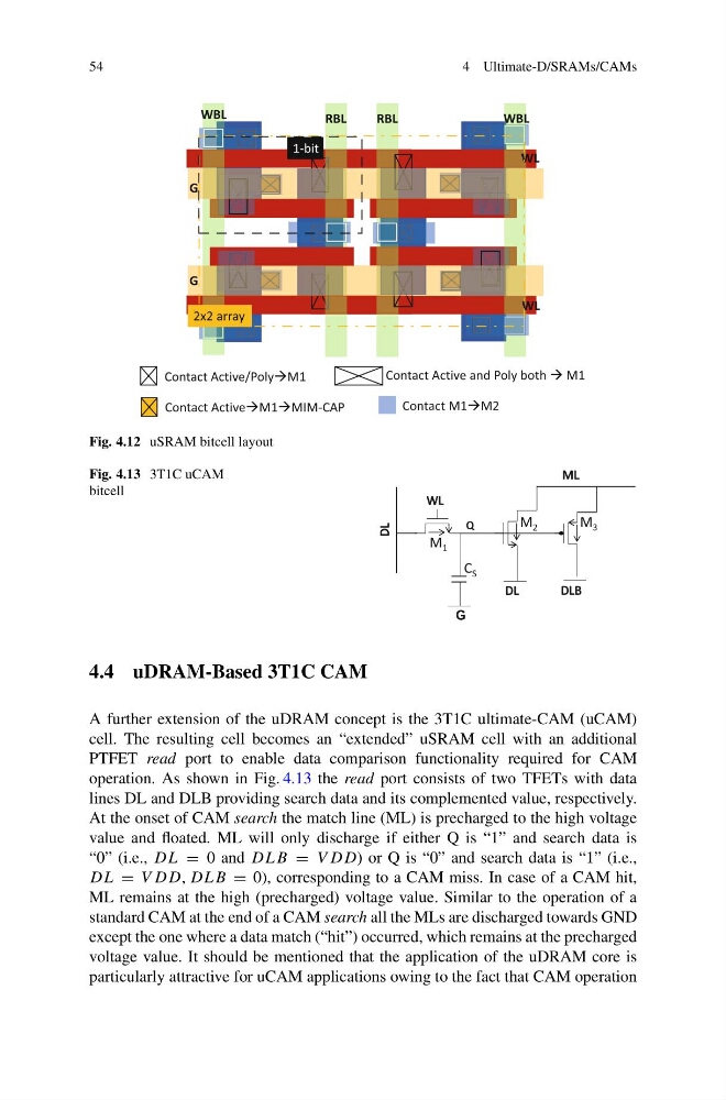
Fig. 4.12 uSRAM bitcell layout
Fig. 4.13 3T1C uCAM
bitcell
G
WL
DL
Q
M 1
C S
DL
M 2
ML
DLB
M 3
4.4 uDRAM-Based 3T1C CAM
A further extension of the uDRAM concept is the 3T1C ultimate-CAM (uCAM)
cell. The resulting cell becomes an “extended” uSRAM cell with an additional
PTFET read port to enable data comparison functionality required for CAM
operation. As shown in Fig. 4.13 the read port consists of two TFETs with data
lines DL and DLB providing search data and its complemented value, respectively.
At the onset of CAM search the match line (ML) is precharged to the high voltage
value and floated. ML will only discharge if either Q is “1” and search data is
“0” (i.e., DL = 0 and DLB = V DD) or Q is “0” and search data is “1” (i.e.,
DL = V DD, DLB = 0), corresponding to a CAM miss. In case of a CAM hit,
ML remains at the high (precharged) voltage value. Similar to the operation of a
standard CAM at the end of a CAM search all the MLs are discharged towards GND
except the one where a data match (“hit”) occurred, which remains at the precharged
voltage value. It should be mentioned that the application of the uDRAM core is
particularly attractive for uCAM applications owing to the fact that CAM operation
4 Ultimate-D/SRAMs/CAMs
RBL
WBL
1-bit
WBL
RBL
2x2 array
Contact Active/PolyM1
Contact M1M2
Contact ActiveM1MIM-CAP
Contact Active and Poly both M1
WL
WL
G
G
Fig. 4.12 uSRAM bitcell layout
Fig. 4.13 3T1C uCAM
bitcell
G
WL
DL
Q
M 1
C S
DL
M 2
ML
DLB
M 3
4.4 uDRAM-Based 3T1C CAM
A further extension of the uDRAM concept is the 3T1C ultimate-CAM (uCAM)
cell. The resulting cell becomes an “extended” uSRAM cell with an additional
PTFET read port to enable data comparison functionality required for CAM
operation. As shown in Fig. 4.13 the read port consists of two TFETs with data
lines DL and DLB providing search data and its complemented value, respectively.
At the onset of CAM search the match line (ML) is precharged to the high voltage
value and floated. ML will only discharge if either Q is “1” and search data is
“0” (i.e., DL = 0 and DLB = V DD) or Q is “0” and search data is “1” (i.e.,
DL = V DD, DLB = 0), corresponding to a CAM miss. In case of a CAM hit,
ML remains at the high (precharged) voltage value. Similar to the operation of a
standard CAM at the end of a CAM search all the MLs are discharged towards GND
except the one where a data match (“hit”) occurred, which remains at the precharged
voltage value. It should be mentioned that the application of the uDRAM core is
particularly attractive for uCAM applications owing to the fact that CAM operation