

4.3 uDRAM-Based 2T1C SRAM
53
WL (read pulse)
c ell node read (storing ‘0’)
RBL read ‘0’
cell node read (storing ‘1’)
RBL read ‘1’
u nselected cell
(storing ‘1’)
u nselected cell
(storing ‘1’)
~326ps
Time [μs]
Voltage [V]
Voltage [V]
1.1
1.0
0.9
0.8
0.7
0.6
0.5
0.4
0.3
0.2
0.1
0.0
–0.1
1.0
0.9
0.8
0.7
0.6
0.5
0.4
0.3
0.2
0.1
0.0
1.9992U
1.9996
2.0000
2.0004
2.0008
2.0012
2.0016
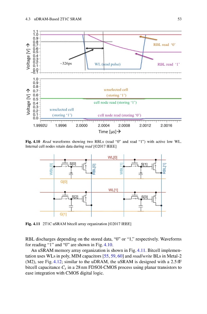
Fig. 4.10 Read waveforms showing two RBLs (read “0” and read “1”) with active low WL.
Internal cell nodes retain data during read [©2017 IEEE]
G[0]
WL[0]
]
0
[
L
B
W
G[1]
WBL[1]
WL[1]
S[0]
S[1]
S[2]
S[3]
[ [ [ [
[ ]
RBL[1]
RBL[0]
Fig. 4.11 2T1C uSRAM bitcell array organization [©2017 IEEE]
RBL discharges depending on the stored data, “0” or “1,” respectively. Waveforms
for reading “1” and “0” are shown in Fig. 4.10.
An uSRAM memory array organization is shown in Fig. 4.11. Bitcell implementation uses WLs in poly, MIM capacitors [55, 59, 60] and read/write BLs in Metal-2
(M2), see Fig. 4.12; similar to the uDRAM, the uSRAM is designed with a 2.5 fF
bitcell capacitance C s in a 28 nm FDSOI-CMOS process using planar transistors to
ease integration with CMOS digital logic.
53
WL (read pulse)
c ell node read (storing ‘0’)
RBL read ‘0’
cell node read (storing ‘1’)
RBL read ‘1’
u nselected cell
(storing ‘1’)
u nselected cell
(storing ‘1’)
~326ps
Time [μs]
Voltage [V]
Voltage [V]
1.1
1.0
0.9
0.8
0.7
0.6
0.5
0.4
0.3
0.2
0.1
0.0
–0.1
1.0
0.9
0.8
0.7
0.6
0.5
0.4
0.3
0.2
0.1
0.0
1.9992U
1.9996
2.0000
2.0004
2.0008
2.0012
2.0016
Fig. 4.10 Read waveforms showing two RBLs (read “0” and read “1”) with active low WL.
Internal cell nodes retain data during read [©2017 IEEE]
G[0]
WL[0]
]
0
[
L
B
W
G[1]
WBL[1]
WL[1]
S[0]
S[1]
S[2]
S[3]
[ [ [ [
[ ]
RBL[1]
RBL[0]
Fig. 4.11 2T1C uSRAM bitcell array organization [©2017 IEEE]
RBL discharges depending on the stored data, “0” or “1,” respectively. Waveforms
for reading “1” and “0” are shown in Fig. 4.10.
An uSRAM memory array organization is shown in Fig. 4.11. Bitcell implementation uses WLs in poly, MIM capacitors [55, 59, 60] and read/write BLs in Metal-2
(M2), see Fig. 4.12; similar to the uDRAM, the uSRAM is designed with a 2.5 fF
bitcell capacitance C s in a 28 nm FDSOI-CMOS process using planar transistors to
ease integration with CMOS digital logic.