

52
4 Ultimate-D/SRAMs/CAMs
reduced by up to 48× without using NWL and thick EOT for capacitor. Array
dynamic power consumption during write is increased by 23% in comparison to
standard CMOS DRAM mainly due to the switching of the virtual ground. However,
the increase in dynamic power consumption is more than compensated by the energy
gain due to refresh-free operation. Moreover, up to 18% throughput can be gained
in comparison to standard CMOS DRAM due to refresh-free operation when used
in a Dual-Data Rate (DDR) memory.
It should be noted that the explanation in this section uses specific voltages on
signals as an example; these voltages can be tuned without any limitation to match
the system requirements. The minimum requirement of the proposed uDRAM
design is to have three supply voltages, i.e. low, medium, and high supply voltages,
such as 0, 0.5 and 1.5 V.
4.3 uDRAM-Based 2T1C SRAM
Writing back the data in eDRAMs when replacing SRAMs close to computeintensive blocks such as CPU, GPU or DSP is a major constraint. Therefore,
eDRAMs are used as big-size L2 cache or lower in the memory hierarchy. In order
to avoid a write-back during a read, another variant of the uDRAM, the ultimateSRAM (uSRAM) [64], which works similarly to an SRAM is proposed. A 2T1C
uSRAM implementation, which can be utilized to replace standard SRAMs to
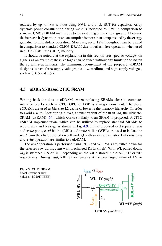
reduce area and leakage is shown in Fig. 4.9. In the proposed cell separate read
and write ports, read bitline (RBL) and write bitline (WBL) are used to isolate the
read from the charge stored on cell node Q with an extra transistor. Data retention
and write operation are similar to a uDRAM.
The read operation is performed using RBL and WL. WLs are pulled down for
the selected row during read with precharged RBLs (high). With WL pulled down,
M 2 is switched ON or OFF depending on the value stored in the cell, “1” or “0,”
respectively. During read, RBL either remains at the precharged value of 1 V or
Fig. 4.9 2T1C uSRAM
bitcell (retention bias
voltages) [©2017 IEEE]
G=0.5V (medium)
WL=1V (high)
V
0
=
L
B
W
)
w
o
l
(
Q=0/0.5V
(low/medium)
M 1
C S
I
CAPL
I NDR or I OFF
Q
(l ( / di )
WL=1V (high)
M 2
RBL=1V (high)
M 1
M 2
Q=0V/0.5V
4 Ultimate-D/SRAMs/CAMs
reduced by up to 48× without using NWL and thick EOT for capacitor. Array
dynamic power consumption during write is increased by 23% in comparison to
standard CMOS DRAM mainly due to the switching of the virtual ground. However,
the increase in dynamic power consumption is more than compensated by the energy
gain due to refresh-free operation. Moreover, up to 18% throughput can be gained
in comparison to standard CMOS DRAM due to refresh-free operation when used
in a Dual-Data Rate (DDR) memory.
It should be noted that the explanation in this section uses specific voltages on
signals as an example; these voltages can be tuned without any limitation to match
the system requirements. The minimum requirement of the proposed uDRAM
design is to have three supply voltages, i.e. low, medium, and high supply voltages,
such as 0, 0.5 and 1.5 V.
4.3 uDRAM-Based 2T1C SRAM
Writing back the data in eDRAMs when replacing SRAMs close to computeintensive blocks such as CPU, GPU or DSP is a major constraint. Therefore,
eDRAMs are used as big-size L2 cache or lower in the memory hierarchy. In order
to avoid a write-back during a read, another variant of the uDRAM, the ultimateSRAM (uSRAM) [64], which works similarly to an SRAM is proposed. A 2T1C
uSRAM implementation, which can be utilized to replace standard SRAMs to
reduce area and leakage is shown in Fig. 4.9. In the proposed cell separate read
and write ports, read bitline (RBL) and write bitline (WBL) are used to isolate the
read from the charge stored on cell node Q with an extra transistor. Data retention
and write operation are similar to a uDRAM.
The read operation is performed using RBL and WL. WLs are pulled down for
the selected row during read with precharged RBLs (high). With WL pulled down,
M 2 is switched ON or OFF depending on the value stored in the cell, “1” or “0,”
respectively. During read, RBL either remains at the precharged value of 1 V or
Fig. 4.9 2T1C uSRAM
bitcell (retention bias
voltages) [©2017 IEEE]
G=0.5V (medium)
WL=1V (high)
V
0
=
L
B
W
)
w
o
l
(
Q=0/0.5V
(low/medium)
M 1
C S
I
CAPL
I NDR or I OFF
Q
(l ( / di )
WL=1V (high)
M 2
RBL=1V (high)
M 1
M 2
Q=0V/0.5V