

4.2 The Ultimate-DRAM (uDRAM): TFET. . .
51
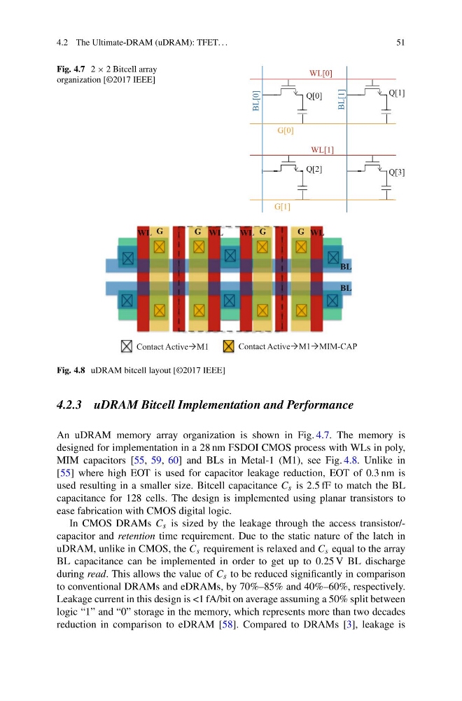
Fig. 4.7 2 × 2 Bitcell array
organization [©2017 IEEE]
G[0]
WL[0]
BL[0]
G[1]
BL[1]
WL[1]
Q[0]
Q[1]
Q[2]
Q[3]
Contact ActiveM1
Contact ActiveM1MIM-CAP
BL
BL
WL
WL
WL
WL
G
G
G
G
Fig. 4.8 uDRAM bitcell layout [©2017 IEEE]
4.2.3 uDRAM Bitcell Implementation and Performance
An uDRAM memory array organization is shown in Fig. 4.7. The memory is
designed for implementation in a 28 nm FSDOI CMOS process with WLs in poly,
MIM capacitors [55, 59, 60] and BLs in Metal-1 (M1), see Fig. 4.8. Unlike in
[55] where high EOT is used for capacitor leakage reduction, EOT of 0.3 nm is
used resulting in a smaller size. Bitcell capacitance C s is 2.5 fF to match the BL
capacitance for 128 cells. The design is implemented using planar transistors to
ease fabrication with CMOS digital logic.
In CMOS DRAMs C s is sized by the leakage through the access transistor/capacitor and retention time requirement. Due to the static nature of the latch in
uDRAM, unlike in CMOS, the C s requirement is relaxed and C s equal to the array
BL capacitance can be implemented in order to get up to 0.25 V BL discharge
during read. This allows the value of C s to be reduced significantly in comparison
to conventional DRAMs and eDRAMs, by 70%–85% and 40%–60%, respectively.
Leakage current in this design is <1 fA/bit on average assuming a 50% split between
logic “1” and “0” storage in the memory, which represents more than two decades
reduction in comparison to eDRAM [58]. Compared to DRAMs [3], leakage is
51
Fig. 4.7 2 × 2 Bitcell array
organization [©2017 IEEE]
G[0]
WL[0]
BL[0]
G[1]
BL[1]
WL[1]
Q[0]
Q[1]
Q[2]
Q[3]
Contact ActiveM1
Contact ActiveM1MIM-CAP
BL
BL
WL
WL
WL
WL
G
G
G
G
Fig. 4.8 uDRAM bitcell layout [©2017 IEEE]
4.2.3 uDRAM Bitcell Implementation and Performance
An uDRAM memory array organization is shown in Fig. 4.7. The memory is
designed for implementation in a 28 nm FSDOI CMOS process with WLs in poly,
MIM capacitors [55, 59, 60] and BLs in Metal-1 (M1), see Fig. 4.8. Unlike in
[55] where high EOT is used for capacitor leakage reduction, EOT of 0.3 nm is
used resulting in a smaller size. Bitcell capacitance C s is 2.5 fF to match the BL
capacitance for 128 cells. The design is implemented using planar transistors to
ease fabrication with CMOS digital logic.
In CMOS DRAMs C s is sized by the leakage through the access transistor/capacitor and retention time requirement. Due to the static nature of the latch in
uDRAM, unlike in CMOS, the C s requirement is relaxed and C s equal to the array
BL capacitance can be implemented in order to get up to 0.25 V BL discharge
during read. This allows the value of C s to be reduced significantly in comparison
to conventional DRAMs and eDRAMs, by 70%–85% and 40%–60%, respectively.
Leakage current in this design is <1 fA/bit on average assuming a 50% split between
logic “1” and “0” storage in the memory, which represents more than two decades
reduction in comparison to eDRAM [58]. Compared to DRAMs [3], leakage is