

50
4 Ultimate-D/SRAMs/CAMs
G=0.5V
(medium)
WL=1.5V (high)
BL=0.5V
(medium)
G=0.5V
(medium)
WL=0V (low)
BL=0.5
(medium)
a.
b.
Q=0.5/0V
Q=0.5V/0V
Q=0.5V/0V
0.5V
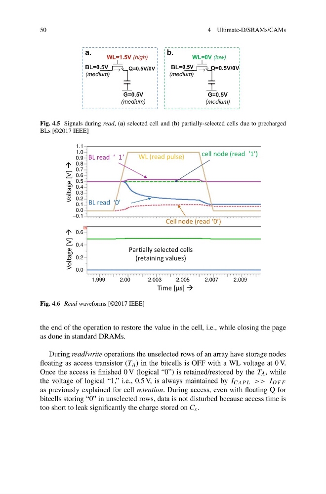
Fig. 4.5 Signals during read, (a) selected cell and (b) partially-selected cells due to precharged
BLs [©2017 IEEE]
WL (read pulse)
Cell node (read ‘0’)
BL read ‘0’
ParƟally selected cells
(retaining values)
cell node (read ‘1’)
BL read ‘ 1’
Time [μs]
Voltage [V]
Voltage [V]
1.1
1.0
0.9
0.8
0.7
0.6
0.5
0.4
0.3
0.2
0.1
0.0
–0.1
0.6
0.4
0.2
0.0
1.999
2.00
2.003
2.005
2.007
2.009
Fig. 4.6 Read waveforms [©2017 IEEE]
the end of the operation to restore the value in the cell, i.e., while closing the page
as done in standard DRAMs.
During read/write operations the unselected rows of an array have storage nodes
floating as access transistor (T A ) in the bitcells is OFF with a WL voltage at 0 V.
Once the access is finished 0 V (logical “0”) is retained/restored by the T A , while
the voltage of logical “1,” i.e., 0.5 V, is always maintained by I CAP L >> I OF F
as previously explained for cell retention. During access, even with floating Q for
bitcells storing “0” in unselected rows, data is not disturbed because access time is
too short to leak significantly the charge stored on C s .
4 Ultimate-D/SRAMs/CAMs
G=0.5V
(medium)
WL=1.5V (high)
BL=0.5V
(medium)
G=0.5V
(medium)
WL=0V (low)
BL=0.5
(medium)
a.
b.
Q=0.5/0V
Q=0.5V/0V
Q=0.5V/0V
0.5V
Fig. 4.5 Signals during read, (a) selected cell and (b) partially-selected cells due to precharged
BLs [©2017 IEEE]
WL (read pulse)
Cell node (read ‘0’)
BL read ‘0’
ParƟally selected cells
(retaining values)
cell node (read ‘1’)
BL read ‘ 1’
Time [μs]
Voltage [V]
Voltage [V]
1.1
1.0
0.9
0.8
0.7
0.6
0.5
0.4
0.3
0.2
0.1
0.0
–0.1
0.6
0.4
0.2
0.0
1.999
2.00
2.003
2.005
2.007
2.009
Fig. 4.6 Read waveforms [©2017 IEEE]
the end of the operation to restore the value in the cell, i.e., while closing the page
as done in standard DRAMs.
During read/write operations the unselected rows of an array have storage nodes
floating as access transistor (T A ) in the bitcells is OFF with a WL voltage at 0 V.
Once the access is finished 0 V (logical “0”) is retained/restored by the T A , while
the voltage of logical “1,” i.e., 0.5 V, is always maintained by I CAP L >> I OF F
as previously explained for cell retention. During access, even with floating Q for
bitcells storing “0” in unselected rows, data is not disturbed because access time is
too short to leak significantly the charge stored on C s .