

4.2 The Ultimate-DRAM (uDRAM): TFET. . .
49
Write pulse
Bitcell reseted (0.5V 0V)
Bitcell set (0V 0.5V)
G0
BL0
BL1
Q[0]
Q[1]
Time [ns]
Voltage [V]
Voltage [V]
Voltage [V]
1.3
1.0
0.7
0.4
0.8
0.5
0.2
-0.1
1.1
1.4
1.0
0.6
0.2
12.0
16.0
20.0
28.0
40.0
36.0
32.0
24.0
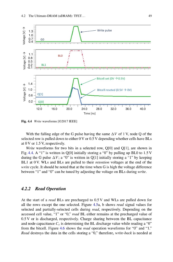
Fig. 4.4 Write waveforms [©2017 IEEE]
With the falling edge of the G pulse having the same V of 1 V, node Q of the
selected row is pulled down to either 0 V or 0.5 V depending whether cells have BLs
at 0 V or 1.5 V, respectively.
Write waveforms for two bits in a selected row, Q[0] and Q[1], are shown in
Fig. 4.4. A “1” is written in Q[0] initially storing a “0” by pulling up BL0 to 1.5 V
during the G pulse V ; a “0” is written in Q[1] initially storing a “1” by keeping
BL1 at 0 V. WLs and BLs are pulled to their retention voltages at the end of the
write cycle. It should be noted that at the time when G is high the voltage difference
between “1” and “0” can be tuned by adjusting the voltage on BLs during write.
4.2.2 Read Operation
At the start of a read BLs are precharged to 0.5 V and WLs are pulled down for
all the rows except the one selected. Figure 4.5a, b shows read signal values for
selected and partially-selected cells during read, respectively. Depending on the
accessed cell value, “1” or “0,” read BL either remains at the precharged value of
0.5 V or is discharged, respectively. Charge sharing between the BL capacitance
and node capacitance C s is determining the BL discharge value while reading a “0”
from the bitcell. Figure 4.6 shows the read operation waveforms for “0” and “1.”
Read destroys the data in the cells storing a “0,” therefore, write-back is needed at
49
Write pulse
Bitcell reseted (0.5V 0V)
Bitcell set (0V 0.5V)
G0
BL0
BL1
Q[0]
Q[1]
Time [ns]
Voltage [V]
Voltage [V]
Voltage [V]
1.3
1.0
0.7
0.4
0.8
0.5
0.2
-0.1
1.1
1.4
1.0
0.6
0.2
12.0
16.0
20.0
28.0
40.0
36.0
32.0
24.0
Fig. 4.4 Write waveforms [©2017 IEEE]
With the falling edge of the G pulse having the same V of 1 V, node Q of the
selected row is pulled down to either 0 V or 0.5 V depending whether cells have BLs
at 0 V or 1.5 V, respectively.
Write waveforms for two bits in a selected row, Q[0] and Q[1], are shown in
Fig. 4.4. A “1” is written in Q[0] initially storing a “0” by pulling up BL0 to 1.5 V
during the G pulse V ; a “0” is written in Q[1] initially storing a “1” by keeping
BL1 at 0 V. WLs and BLs are pulled to their retention voltages at the end of the
write cycle. It should be noted that at the time when G is high the voltage difference
between “1” and “0” can be tuned by adjusting the voltage on BLs during write.
4.2.2 Read Operation
At the start of a read BLs are precharged to 0.5 V and WLs are pulled down for
all the rows except the one selected. Figure 4.5a, b shows read signal values for
selected and partially-selected cells during read, respectively. Depending on the
accessed cell value, “1” or “0,” read BL either remains at the precharged value of
0.5 V or is discharged, respectively. Charge sharing between the BL capacitance
and node capacitance C s is determining the BL discharge value while reading a “0”
from the bitcell. Figure 4.6 shows the read operation waveforms for “0” and “1.”
Read destroys the data in the cells storing a “0,” therefore, write-back is needed at