

48
4 Ultimate-D/SRAMs/CAMs
size is decided only by the bitline capacitance to be able to perform a read; (3)
Unlike the high EOT of the capacitors in [55], which is used to reduce their leakage,
the proposed design uses an EOT of 0.3 nm, which results in reduced area; (4) The
smaller capacitance reduces the cost of the process used for eDRAM implemented
within a single chip with CMOS logic.
4.2.1 Write Operation
Write operation of both “0” and “1” using a single TFET device in the conventional
way of CMOS DRAMs is not possible due to the unidirectional V G -controlled
drain current in TFETs. In the proposed design, a write is performed by thermionic
injection in the reverse-biased TFET (region III, Fig. 4.2) and using capacitive
coupling between the virtual ground G and storage node Q. During write, all WLs
are pulled down except for the one corresponding to the row to be written; BLs are
pulled up or pulled down for writing data having a logical “1” or “0,” respectively.
In case of writing a “1,” once the BL is pulled up the bitcell can be considered as
initialized for write with the Q node rising to approximately 0.5 V regardless of the
state stored before. This occurs due to the fact that with BL set to high voltage the
access transistor T A is in forward conduction and will pull up Q towards BL. After
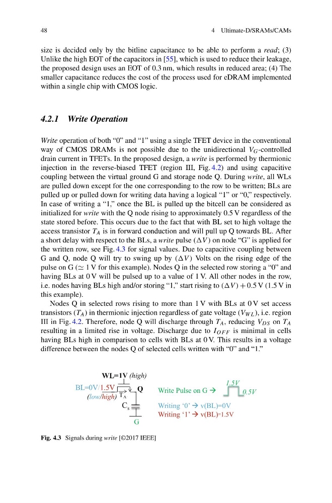
a short delay with respect to the BLs, a write pulse ((V ) on node “G” is applied for
the written row, see Fig. 4.3 for signal values. Due to capacitive coupling between
G and Q, node Q will try to swing up by ((V ) Volts on the rising edge of the
pulse on G ( 1 V for this example). Nodes Q in the selected row storing a “0” and
having BLs at 0 V will be pulsed up to a value of 1 V. All other nodes in the row,
i.e. nodes having BLs high and/or storing “1,” start rising to ((V ) + 0.5 V (1.5 V in
this example).
Nodes Q in selected rows rising to more than 1 V with BLs at 0 V set access
transistors (T A ) in thermionic injection regardless of gate voltage (V W L ), i.e. region
III in Fig. 4.2. Therefore, node Q will discharge through T A , reducing V DS on T A
resulting in a limited rise in voltage. Discharge due to I OF F is minimal in cells
having BLs high in comparison to cells with BLs at 0 V. This results in a voltage
difference between the nodes Q of selected cells written with “0” and “1.”
G
1V (high)
0V/1V
(low/high)
0.5V
1.5V
T A
C s
Write Pulse on G
Writing ‘0’ v(BL)=0V
Writing ‘1’ v(BL)=1V
BL=0V/1.5V
1.5V
WL=
T A
Q
Fig. 4.3 Signals during write [©2017 IEEE]
4 Ultimate-D/SRAMs/CAMs
size is decided only by the bitline capacitance to be able to perform a read; (3)
Unlike the high EOT of the capacitors in [55], which is used to reduce their leakage,
the proposed design uses an EOT of 0.3 nm, which results in reduced area; (4) The
smaller capacitance reduces the cost of the process used for eDRAM implemented
within a single chip with CMOS logic.
4.2.1 Write Operation
Write operation of both “0” and “1” using a single TFET device in the conventional
way of CMOS DRAMs is not possible due to the unidirectional V G -controlled
drain current in TFETs. In the proposed design, a write is performed by thermionic
injection in the reverse-biased TFET (region III, Fig. 4.2) and using capacitive
coupling between the virtual ground G and storage node Q. During write, all WLs
are pulled down except for the one corresponding to the row to be written; BLs are
pulled up or pulled down for writing data having a logical “1” or “0,” respectively.
In case of writing a “1,” once the BL is pulled up the bitcell can be considered as
initialized for write with the Q node rising to approximately 0.5 V regardless of the
state stored before. This occurs due to the fact that with BL set to high voltage the
access transistor T A is in forward conduction and will pull up Q towards BL. After
a short delay with respect to the BLs, a write pulse ((V ) on node “G” is applied for
the written row, see Fig. 4.3 for signal values. Due to capacitive coupling between
G and Q, node Q will try to swing up by ((V ) Volts on the rising edge of the
pulse on G ( 1 V for this example). Nodes Q in the selected row storing a “0” and
having BLs at 0 V will be pulsed up to a value of 1 V. All other nodes in the row,
i.e. nodes having BLs high and/or storing “1,” start rising to ((V ) + 0.5 V (1.5 V in
this example).
Nodes Q in selected rows rising to more than 1 V with BLs at 0 V set access
transistors (T A ) in thermionic injection regardless of gate voltage (V W L ), i.e. region
III in Fig. 4.2. Therefore, node Q will discharge through T A , reducing V DS on T A
resulting in a limited rise in voltage. Discharge due to I OF F is minimal in cells
having BLs high in comparison to cells with BLs at 0 V. This results in a voltage
difference between the nodes Q of selected cells written with “0” and “1.”
G
1V (high)
0V/1V
(low/high)
0.5V
1.5V
T A
C s
Write Pulse on G
Writing ‘0’ v(BL)=0V
Writing ‘1’ v(BL)=1V
BL=0V/1.5V
1.5V
WL=
T A
Q
Fig. 4.3 Signals during write [©2017 IEEE]