

40
3 SRAMs
Bit-0
Bit-1
Cell and Array
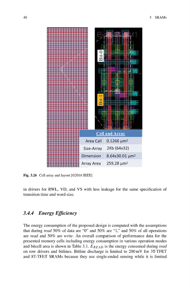
Area Call 0.1266 μm 2
Size-Array 2Kb (64x32)
Dimension 8.64x30.01 μm 2
Array Area 259.28 μm 2
Fig. 3.26 Cell array and layout [©2016 IEEE]
in drivers for RWL, VD, and VS with less leakage for the same specification of
transition time and word size.
3.4.4 Energy Efficiency
The energy consumption of the proposed design is computed with the assumptions
that during read 50% of data are “0” and 50% are “1,” and 50% of all operations
are read and 50% are write. An overall comparison of performance data for the
presented memory cells including energy consumption in various operation modes
and bitcell area is shown in Table 3.1. E READ is the energy consumed during read
on row drivers and bitlines. Bitline discharge is limited to 200 mV for 3T-TFET
and 8T-TFET SRAMs because they use single-ended sensing while it is limited
3 SRAMs
Bit-0
Bit-1
Cell and Array
Area Call 0.1266 μm 2
Size-Array 2Kb (64x32)
Dimension 8.64x30.01 μm 2
Array Area 259.28 μm 2
Fig. 3.26 Cell array and layout [©2016 IEEE]
in drivers for RWL, VD, and VS with less leakage for the same specification of
transition time and word size.
3.4.4 Energy Efficiency
The energy consumption of the proposed design is computed with the assumptions
that during read 50% of data are “0” and 50% are “1,” and 50% of all operations
are read and 50% are write. An overall comparison of performance data for the
presented memory cells including energy consumption in various operation modes
and bitcell area is shown in Table 3.1. E READ is the energy consumed during read
on row drivers and bitlines. Bitline discharge is limited to 200 mV for 3T-TFET
and 8T-TFET SRAMs because they use single-ended sensing while it is limited