

38
3 SRAMs
Fig. 3.23 Read operation
waveform [©2016 IEEE]
0.0
0.1
0.2
0.3
0.4
0.5
0.6
0.7
0.8
0.0
2.0
4.0
6.0
8.0
10.0 12.0 14.0
V(RBL [0])-Read 0
V(RBL [0])-Read 1
V(RWL [0])
Time [ns]
Voltage [V]
BiasM0[0]
BiasM1[0]
BiasM0[n-1]
VD[0]
VS[0]
BiasM1[n-1]
RWL[0]
RBL[0]
RWL[m-1]
RBL[n-1]
VD[m-1]
VS[m-1]
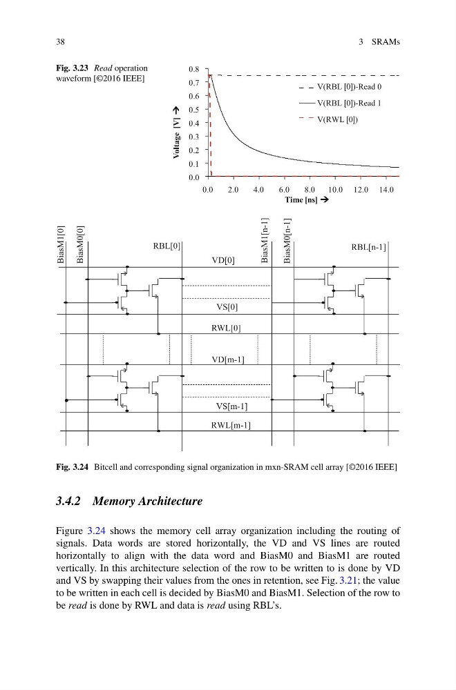
Fig. 3.24 Bitcell and corresponding signal organization in mxn-SRAM cell array [©2016 IEEE]
3.4.2 Memory Architecture
Figure 3.24 shows the memory cell array organization including the routing of
signals. Data words are stored horizontally, the VD and VS lines are routed
horizontally to align with the data word and BiasM0 and BiasM1 are routed
vertically. In this architecture selection of the row to be written to is done by VD
and VS by swapping their values from the ones in retention, see Fig. 3.21; the value
to be written in each cell is decided by BiasM0 and BiasM1. Selection of the row to
be read is done by RWL and data is read using RBL’s.
3 SRAMs
Fig. 3.23 Read operation
waveform [©2016 IEEE]
0.0
0.1
0.2
0.3
0.4
0.5
0.6
0.7
0.8
0.0
2.0
4.0
6.0
8.0
10.0 12.0 14.0
V(RBL [0])-Read 0
V(RBL [0])-Read 1
V(RWL [0])
Time [ns]
Voltage [V]
BiasM0[0]
BiasM1[0]
BiasM0[n-1]
VD[0]
VS[0]
BiasM1[n-1]
RWL[0]
RBL[0]
RWL[m-1]
RBL[n-1]
VD[m-1]
VS[m-1]
Fig. 3.24 Bitcell and corresponding signal organization in mxn-SRAM cell array [©2016 IEEE]
3.4.2 Memory Architecture
Figure 3.24 shows the memory cell array organization including the routing of
signals. Data words are stored horizontally, the VD and VS lines are routed
horizontally to align with the data word and BiasM0 and BiasM1 are routed
vertically. In this architecture selection of the row to be written to is done by VD
and VS by swapping their values from the ones in retention, see Fig. 3.21; the value
to be written in each cell is decided by BiasM0 and BiasM1. Selection of the row to
be read is done by RWL and data is read using RBL’s.