

3.4 3T-TFET Bitcell-Based TFET-CMOS Hybrid Memory
37
Time [ns]
Voltage [V]
Voltage [V]
0.0
0.2
0.4
0.6
0.8
1.0
0 2 4 6 8 10 12 14 16 18 20 22 24 26 28
V(BiasM0[0])
V(BiasM1[0])
0.2
0.3
0.4
0.5
0.6
0.7
0.8
0.9
0 2 4 6 8 10 12 14 16 18 20 22 24 26 28
V(VS[0])
V(VD[0])
V(Q[0])
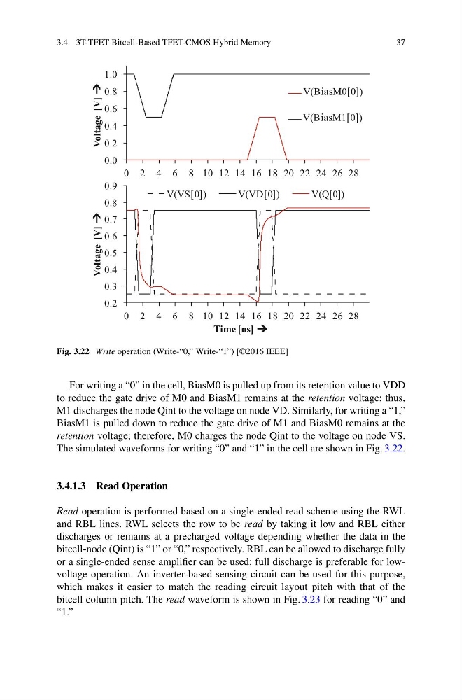
Fig. 3.22 Write operation (Write-“0,” Write-“1”) [©2016 IEEE]
For writing a “0” in the cell, BiasM0 is pulled up from its retention value to VDD
to reduce the gate drive of M0 and BiasM1 remains at the retention voltage; thus,
M1 discharges the node Qint to the voltage on node VD. Similarly, for writing a “1,”
BiasM1 is pulled down to reduce the gate drive of M1 and BiasM0 remains at the
retention voltage; therefore, M0 charges the node Qint to the voltage on node VS.
The simulated waveforms for writing “0” and “1” in the cell are shown in Fig. 3.22.
3.4.1.3 Read Operation
Read operation is performed based on a single-ended read scheme using the RWL
and RBL lines. RWL selects the row to be read by taking it low and RBL either
discharges or remains at a precharged voltage depending whether the data in the
bitcell-node (Qint) is “1” or “0,” respectively. RBL can be allowed to discharge fully
or a single-ended sense amplifier can be used; full discharge is preferable for lowvoltage operation. An inverter-based sensing circuit can be used for this purpose,
which makes it easier to match the reading circuit layout pitch with that of the
bitcell column pitch. The read waveform is shown in Fig. 3.23 for reading “0” and
“1.”
37
Time [ns]
Voltage [V]
Voltage [V]
0.0
0.2
0.4
0.6
0.8
1.0
0 2 4 6 8 10 12 14 16 18 20 22 24 26 28
V(BiasM0[0])
V(BiasM1[0])
0.2
0.3
0.4
0.5
0.6
0.7
0.8
0.9
0 2 4 6 8 10 12 14 16 18 20 22 24 26 28
V(VS[0])
V(VD[0])
V(Q[0])
Fig. 3.22 Write operation (Write-“0,” Write-“1”) [©2016 IEEE]
For writing a “0” in the cell, BiasM0 is pulled up from its retention value to VDD
to reduce the gate drive of M0 and BiasM1 remains at the retention voltage; thus,
M1 discharges the node Qint to the voltage on node VD. Similarly, for writing a “1,”
BiasM1 is pulled down to reduce the gate drive of M1 and BiasM0 remains at the
retention voltage; therefore, M0 charges the node Qint to the voltage on node VS.
The simulated waveforms for writing “0” and “1” in the cell are shown in Fig. 3.22.
3.4.1.3 Read Operation
Read operation is performed based on a single-ended read scheme using the RWL
and RBL lines. RWL selects the row to be read by taking it low and RBL either
discharges or remains at a precharged voltage depending whether the data in the
bitcell-node (Qint) is “1” or “0,” respectively. RBL can be allowed to discharge fully
or a single-ended sense amplifier can be used; full discharge is preferable for lowvoltage operation. An inverter-based sensing circuit can be used for this purpose,
which makes it easier to match the reading circuit layout pitch with that of the
bitcell column pitch. The read waveform is shown in Fig. 3.23 for reading “0” and
“1.”