

36
3 SRAMs
2VDD
VDDL
VDDH
VDD
Qint
V GS > 0
V GS –V OFF 0
I
D =I
ON
I
D 0
VDD
VDDL
VDDH
GND
Qint
V GS <0
I
D =0
I
D =I
ON
2VDD
VDDH
VDDL
GND
Qint
V GS > 0
V GS < 0
V DS <= 0
V DS >= 0
Retention
Write ‘0’
Write ‘1’
VDDL
VDDH
Qint
I
D =I
ON
I
D 0
VDDL
VDDH
Qint
I
D 0
I
D -->I
ON
2VDD
VDDH
VDDL
GND
Qint
V GS >= 0
V GS < =0
V DS >= 0
V DS <= 0
V GS –V OFF 0
V GS < =0
GND
VDD
V GS –V OFF 0
V GS –V OFF 0
V GS < =0
2VDD
VDD
Arch.-1
Arch.-2
GND < VDDL < VDD < VDDH < 2VDD
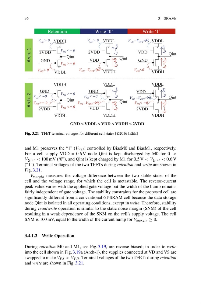
Fig. 3.21 TFET terminal voltages for different cell states [©2016 IEEE]
and M1 preserves the “1” (V V D ) controlled by BiasM0 and BiasM1, respectively.
For a cell supply VDD = 0.6 V node Qint is kept discharged by M0 for 0 <
V Qint < 100 mV (‘0”), and Qint is kept charged by M1 for 0.5 V < V Qint < 0.6 V
(“1”). Terminal voltages of the two TFETs during retention and write are shown in
Fig. 3.21.
V margin measures the voltage difference between the two stable states of the
cell and the voltage range, for which the cell is metastable. The reverse-current
peak value varies with the applied gate voltage but the width of the hump remains
fairly independent of gate voltage. The stability constraints for the proposed cell are
significantly different from a conventional 6T-SRAM cell because the data storage
node Qint is isolated in all operating conditions, except in write. Therefore, stability
during read/write operation is similar to the static noise margin (SNM) of the cell
resulting in a weak dependence of the SNM on the cell’s supply voltage. The cell
SNM is 100 mV, equal to the width of the current hump for V margin ≥ 0.
3.4.1.2 Write Operation
During retention M0 and M1, see Fig. 3.19, are reverse biased; in order to write
into the cell shown in Fig. 3.19a (Arch-1), the supplies connected at VD and VS are
swapped to make V V S > V V D . Terminal voltages of the two TFETs during retention
and write are shown in Fig. 3.21.
3 SRAMs
2VDD
VDDL
VDDH
VDD
Qint
V GS > 0
V GS –V OFF 0
I
D =I
ON
I
D 0
VDD
VDDL
VDDH
GND
Qint
V GS <0
I
D =0
I
D =I
ON
2VDD
VDDH
VDDL
GND
Qint
V GS > 0
V GS < 0
V DS <= 0
V DS >= 0
Retention
Write ‘0’
Write ‘1’
VDDL
VDDH
Qint
I
D =I
ON
I
D 0
VDDL
VDDH
Qint
I
D 0
I
D -->I
ON
2VDD
VDDH
VDDL
GND
Qint
V GS >= 0
V GS < =0
V DS >= 0
V DS <= 0
V GS –V OFF 0
V GS < =0
GND
VDD
V GS –V OFF 0
V GS –V OFF 0
V GS < =0
2VDD
VDD
Arch.-1
Arch.-2
GND < VDDL < VDD < VDDH < 2VDD
Fig. 3.21 TFET terminal voltages for different cell states [©2016 IEEE]
and M1 preserves the “1” (V V D ) controlled by BiasM0 and BiasM1, respectively.
For a cell supply VDD = 0.6 V node Qint is kept discharged by M0 for 0 <
V Qint < 100 mV (‘0”), and Qint is kept charged by M1 for 0.5 V < V Qint < 0.6 V
(“1”). Terminal voltages of the two TFETs during retention and write are shown in
Fig. 3.21.
V margin measures the voltage difference between the two stable states of the
cell and the voltage range, for which the cell is metastable. The reverse-current
peak value varies with the applied gate voltage but the width of the hump remains
fairly independent of gate voltage. The stability constraints for the proposed cell are
significantly different from a conventional 6T-SRAM cell because the data storage
node Qint is isolated in all operating conditions, except in write. Therefore, stability
during read/write operation is similar to the static noise margin (SNM) of the cell
resulting in a weak dependence of the SNM on the cell’s supply voltage. The cell
SNM is 100 mV, equal to the width of the current hump for V margin ≥ 0.
3.4.1.2 Write Operation
During retention M0 and M1, see Fig. 3.19, are reverse biased; in order to write
into the cell shown in Fig. 3.19a (Arch-1), the supplies connected at VD and VS are
swapped to make V V S > V V D . Terminal voltages of the two TFETs during retention
and write are shown in Fig. 3.21.