

3.3 Dual-Port SRAM Architecture
33
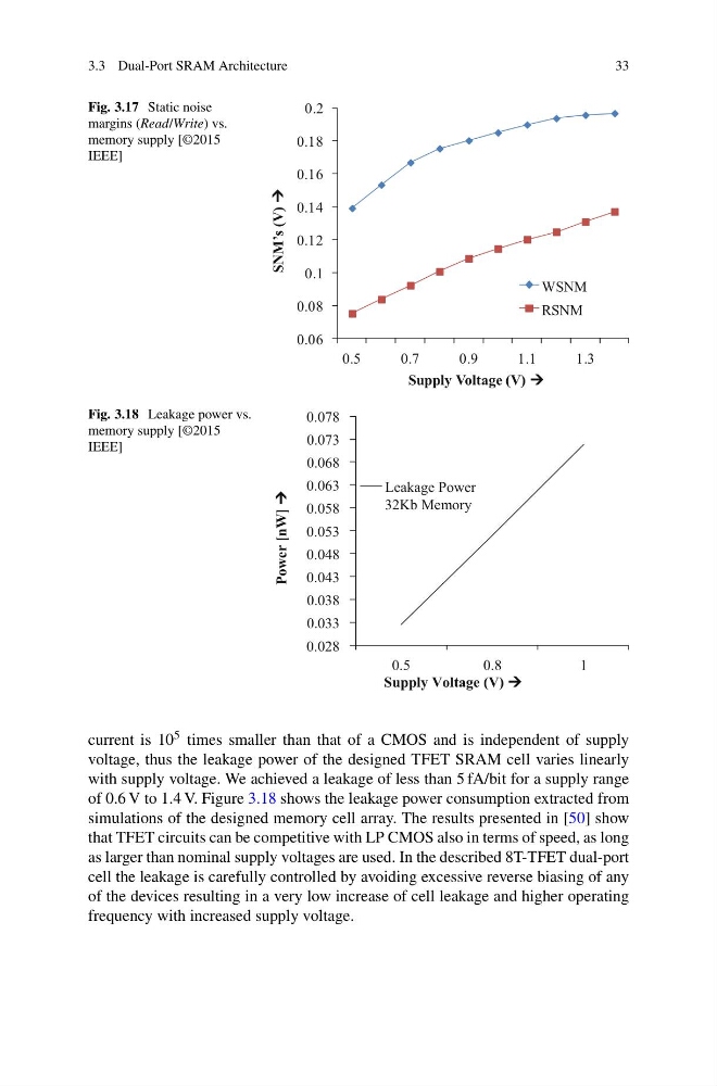
Fig. 3.17 Static noise
margins (Read/Write) vs.
memory supply [©2015
IEEE]
0.06
0.08
0.1
0.12
0.14
0.16
0.18
0.2
0.5
0.7
0.9
1.1
1.3
WSNM
RSNM
SNM’s (V)
Supply Voltage (V)
Fig. 3.18 Leakage power vs.
memory supply [©2015
IEEE]
Power [nW]
Supply Voltage (V)
0.028
0.033
0.038
0.043
0.048
0.053
0.058
0.063
0.068
0.073
0.078
0.5
0.8
1
Leakage Power
32Kb Memory
current is 10 5 times smaller than that of a CMOS and is independent of supply
voltage, thus the leakage power of the designed TFET SRAM cell varies linearly
with supply voltage. We achieved a leakage of less than 5 fA/bit for a supply range
of 0.6 V to 1.4 V. Figure 3.18 shows the leakage power consumption extracted from
simulations of the designed memory cell array. The results presented in [50] show
that TFET circuits can be competitive with LP CMOS also in terms of speed, as long
as larger than nominal supply voltages are used. In the described 8T-TFET dual-port
cell the leakage is carefully controlled by avoiding excessive reverse biasing of any
of the devices resulting in a very low increase of cell leakage and higher operating
frequency with increased supply voltage.
33
Fig. 3.17 Static noise
margins (Read/Write) vs.
memory supply [©2015
IEEE]
0.06
0.08
0.1
0.12
0.14
0.16
0.18
0.2
0.5
0.7
0.9
1.1
1.3
WSNM
RSNM
SNM’s (V)
Supply Voltage (V)
Fig. 3.18 Leakage power vs.
memory supply [©2015
IEEE]
Power [nW]
Supply Voltage (V)
0.028
0.033
0.038
0.043
0.048
0.053
0.058
0.063
0.068
0.073
0.078
0.5
0.8
1
Leakage Power
32Kb Memory
current is 10 5 times smaller than that of a CMOS and is independent of supply
voltage, thus the leakage power of the designed TFET SRAM cell varies linearly
with supply voltage. We achieved a leakage of less than 5 fA/bit for a supply range
of 0.6 V to 1.4 V. Figure 3.18 shows the leakage power consumption extracted from
simulations of the designed memory cell array. The results presented in [50] show
that TFET circuits can be competitive with LP CMOS also in terms of speed, as long
as larger than nominal supply voltages are used. In the described 8T-TFET dual-port
cell the leakage is carefully controlled by avoiding excessive reverse biasing of any
of the devices resulting in a very low increase of cell leakage and higher operating
frequency with increased supply voltage.