

3.3 Dual-Port SRAM Architecture
31
-0.3
-0.1
0.1
0.3
0.5
0.7
0.9
0.0 0.6 1.2 1.8 2.4 3.0 3.6 4.2 4.8 5.4 6.0 6.6
. V(WL1)
V(TFET CELL.V2)
V(TFET CELL.V1)
Voltage (V)
Time (ns)
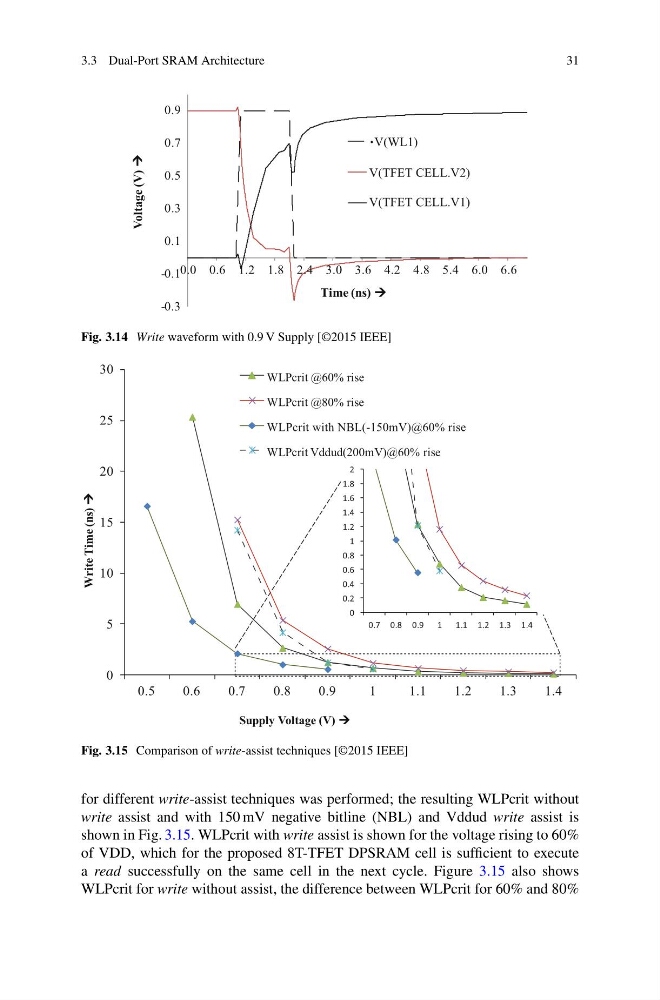
Fig. 3.14 Write waveform with 0.9 V Supply [©2015 IEEE]
Write Time (ns)
Supply Voltage (V)
0
0.2
0.4
0.6
0.8
1
1.2
1.4
1.6
1.8
2
0.7 0.8 0.9 1 1.1 1.2 1.3 1.4
0
5
10
15
20
25
30
0.5
0.6
0.7
0.8
0.9
1
1.1
1.2
1.3
1.4
WLPcrit @60% rise
WLPcrit @80% rise
WLPcrit with NBL(-150mV)@60% rise
WLPcrit Vddud(200mV)@60% rise
Fig. 3.15 Comparison of write-assist techniques [©2015 IEEE]
for different write-assist techniques was performed; the resulting WLPcrit without
write assist and with 150 mV negative bitline (NBL) and Vddud write assist is
shown in Fig. 3.15. WLPcrit with write assist is shown for the voltage rising to 60%
of VDD, which for the proposed 8T-TFET DPSRAM cell is sufficient to execute
a read successfully on the same cell in the next cycle. Figure 3.15 also shows
WLPcrit for write without assist, the difference between WLPcrit for 60% and 80%
31
-0.3
-0.1
0.1
0.3
0.5
0.7
0.9
0.0 0.6 1.2 1.8 2.4 3.0 3.6 4.2 4.8 5.4 6.0 6.6
. V(WL1)
V(TFET CELL.V2)
V(TFET CELL.V1)
Voltage (V)
Time (ns)
Fig. 3.14 Write waveform with 0.9 V Supply [©2015 IEEE]
Write Time (ns)
Supply Voltage (V)
0
0.2
0.4
0.6
0.8
1
1.2
1.4
1.6
1.8
2
0.7 0.8 0.9 1 1.1 1.2 1.3 1.4
0
5
10
15
20
25
30
0.5
0.6
0.7
0.8
0.9
1
1.1
1.2
1.3
1.4
WLPcrit @60% rise
WLPcrit @80% rise
WLPcrit with NBL(-150mV)@60% rise
WLPcrit Vddud(200mV)@60% rise
Fig. 3.15 Comparison of write-assist techniques [©2015 IEEE]
for different write-assist techniques was performed; the resulting WLPcrit without
write assist and with 150 mV negative bitline (NBL) and Vddud write assist is
shown in Fig. 3.15. WLPcrit with write assist is shown for the voltage rising to 60%
of VDD, which for the proposed 8T-TFET DPSRAM cell is sufficient to execute
a read successfully on the same cell in the next cycle. Figure 3.15 also shows
WLPcrit for write without assist, the difference between WLPcrit for 60% and 80%