

3.3 Dual-Port SRAM Architecture
29
Muxes-8x1
WL Drivers
Row Dec.
SA[0-63]
BLR1[0-255]
&
BLR2[0-255]
BL Drivers
Column[n]-128x1
Column[n+7]-128x1
TFET
SRAM
Array
128x256
Cell
[0]
Cell
[127]
BLR1
BLR2
BLW1
BLW2
WL1[0]
WL2[0]
WL1[127]
WL2[127]
BLR1
SA
2-Muxes-8x1
BLR2
SA
Port1
Port2
Write Logic
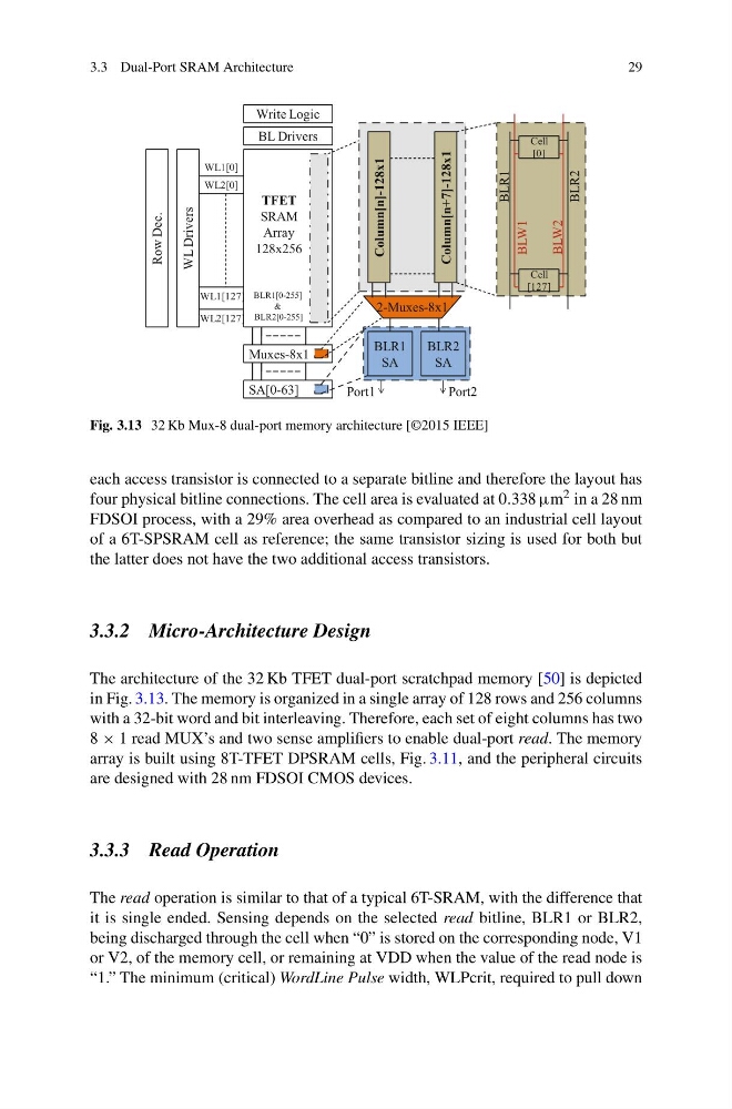
Fig. 3.13 32 Kb Mux-8 dual-port memory architecture [©2015 IEEE]
each access transistor is connected to a separate bitline and therefore the layout has
four physical bitline connections. The cell area is evaluated at 0.338 µm 2 in a 28 nm
FDSOI process, with a 29% area overhead as compared to an industrial cell layout
of a 6T-SPSRAM cell as reference; the same transistor sizing is used for both but
the latter does not have the two additional access transistors.
3.3.2 Micro-Architecture Design
The architecture of the 32 Kb TFET dual-port scratchpad memory [50] is depicted
in Fig. 3.13. The memory is organized in a single array of 128 rows and 256 columns
with a 32-bit word and bit interleaving. Therefore, each set of eight columns has two
8 × 1 read MUX’s and two sense amplifiers to enable dual-port read. The memory
array is built using 8T-TFET DPSRAM cells, Fig. 3.11, and the peripheral circuits
are designed with 28 nm FDSOI CMOS devices.
3.3.3 Read Operation
The read operation is similar to that of a typical 6T-SRAM, with the difference that
it is single ended. Sensing depends on the selected read bitline, BLR1 or BLR2,
being discharged through the cell when “0” is stored on the corresponding node, V1
or V2, of the memory cell, or remaining at VDD when the value of the read node is
“1.” The minimum (critical) WordLine Pulse width, WLPcrit, required to pull down
29
Muxes-8x1
WL Drivers
Row Dec.
SA[0-63]
BLR1[0-255]
&
BLR2[0-255]
BL Drivers
Column[n]-128x1
Column[n+7]-128x1
TFET
SRAM
Array
128x256
Cell
[0]
Cell
[127]
BLR1
BLR2
BLW1
BLW2
WL1[0]
WL2[0]
WL1[127]
WL2[127]
BLR1
SA
2-Muxes-8x1
BLR2
SA
Port1
Port2
Write Logic
Fig. 3.13 32 Kb Mux-8 dual-port memory architecture [©2015 IEEE]
each access transistor is connected to a separate bitline and therefore the layout has
four physical bitline connections. The cell area is evaluated at 0.338 µm 2 in a 28 nm
FDSOI process, with a 29% area overhead as compared to an industrial cell layout
of a 6T-SPSRAM cell as reference; the same transistor sizing is used for both but
the latter does not have the two additional access transistors.
3.3.2 Micro-Architecture Design
The architecture of the 32 Kb TFET dual-port scratchpad memory [50] is depicted
in Fig. 3.13. The memory is organized in a single array of 128 rows and 256 columns
with a 32-bit word and bit interleaving. Therefore, each set of eight columns has two
8 × 1 read MUX’s and two sense amplifiers to enable dual-port read. The memory
array is built using 8T-TFET DPSRAM cells, Fig. 3.11, and the peripheral circuits
are designed with 28 nm FDSOI CMOS devices.
3.3.3 Read Operation
The read operation is similar to that of a typical 6T-SRAM, with the difference that
it is single ended. Sensing depends on the selected read bitline, BLR1 or BLR2,
being discharged through the cell when “0” is stored on the corresponding node, V1
or V2, of the memory cell, or remaining at VDD when the value of the read node is
“1.” The minimum (critical) WordLine Pulse width, WLPcrit, required to pull down