

28
3 SRAMs
BLW1
VDD
2
R
L
B
BLR1
BLW2
WL2
WL2
WL1
WL1
V2
V1
TR3
TR4
TR1
TR2
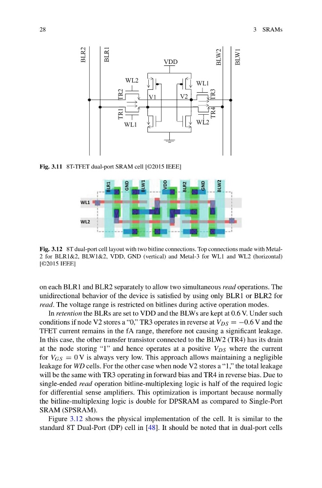
Fig. 3.11 8T-TFET dual-port SRAM cell [©2015 IEEE]
BLR1
GND
BLW1
VDD
BLR2
GND
BLW2
WL1
WL2
Fig. 3.12 8T dual-port cell layout with two bitline connections. Top connections made with Metal2 for BLR1&2, BLW1&2, VDD, GND (vertical) and Metal-3 for WL1 and WL2 (horizontal)
[©2015 IEEE]
on each BLR1 and BLR2 separately to allow two simultaneous read operations. The
unidirectional behavior of the device is satisfied by using only BLR1 or BLR2 for
read. The voltage range is restricted on bitlines during active operation modes.
In retention the BLRs are set to VDD and the BLWs are kept at 0.6 V. Under such
conditions if node V2 stores a “0,” TR3 operates in reverse at V DS = −0.6 V and the
TFET current remains in the fA range, therefore not causing a significant leakage.
In this case, the other transfer transistor connected to the BLW2 (TR4) has its drain
at the node storing “1” and hence operates at a positive V DS where the current
for V GS = 0 V is always very low. This approach allows maintaining a negligible
leakage for WD cells. For the other case when node V2 stores a “1,” the total leakage
will be the same with TR3 operating in forward bias and TR4 in reverse bias. Due to
single-ended read operation bitline-multiplexing logic is half of the required logic
for differential sense amplifiers. This optimization is important because normally
the bitline-multiplexing logic is double for DPSRAM as compared to Single-Port
SRAM (SPSRAM).
Figure 3.12 shows the physical implementation of the cell. It is similar to the
standard 8T Dual-Port (DP) cell in [48]. It should be noted that in dual-port cells
3 SRAMs
BLW1
VDD
2
R
L
B
BLR1
BLW2
WL2
WL2
WL1
WL1
V2
V1
TR3
TR4
TR1
TR2
Fig. 3.11 8T-TFET dual-port SRAM cell [©2015 IEEE]
BLR1
GND
BLW1
VDD
BLR2
GND
BLW2
WL1
WL2
Fig. 3.12 8T dual-port cell layout with two bitline connections. Top connections made with Metal2 for BLR1&2, BLW1&2, VDD, GND (vertical) and Metal-3 for WL1 and WL2 (horizontal)
[©2015 IEEE]
on each BLR1 and BLR2 separately to allow two simultaneous read operations. The
unidirectional behavior of the device is satisfied by using only BLR1 or BLR2 for
read. The voltage range is restricted on bitlines during active operation modes.
In retention the BLRs are set to VDD and the BLWs are kept at 0.6 V. Under such
conditions if node V2 stores a “0,” TR3 operates in reverse at V DS = −0.6 V and the
TFET current remains in the fA range, therefore not causing a significant leakage.
In this case, the other transfer transistor connected to the BLW2 (TR4) has its drain
at the node storing “1” and hence operates at a positive V DS where the current
for V GS = 0 V is always very low. This approach allows maintaining a negligible
leakage for WD cells. For the other case when node V2 stores a “1,” the total leakage
will be the same with TR3 operating in forward bias and TR4 in reverse bias. Due to
single-ended read operation bitline-multiplexing logic is half of the required logic
for differential sense amplifiers. This optimization is important because normally
the bitline-multiplexing logic is double for DPSRAM as compared to Single-Port
SRAM (SPSRAM).
Figure 3.12 shows the physical implementation of the cell. It is similar to the
standard 8T Dual-Port (DP) cell in [48]. It should be noted that in dual-port cells