

24
3 SRAMs
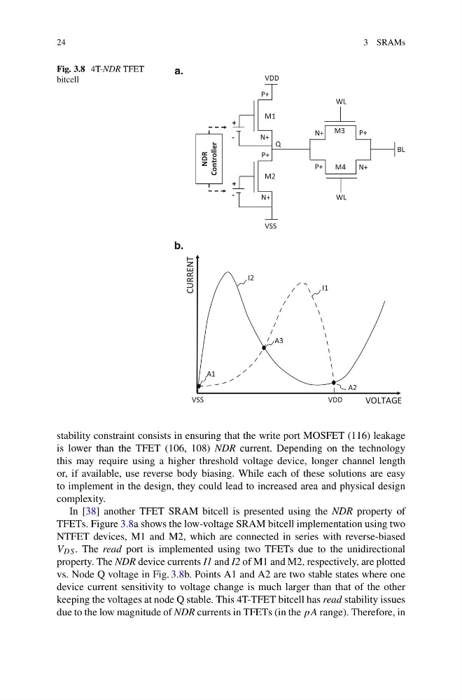
Fig. 3.8 4T-NDR TFET
bitcell
a.
b.
+
+
-
-
N+
N+
P+
P+
NDR
Controller
M1
M2
N+
P+
N+
P+
WL
WL
VDD
VSS
M4
M3
BL
VSS
VDD
A1
A3
A2
T
N
E
R
R
U
C
VOLTAGE
I2
I1
Q
stability constraint consists in ensuring that the write port MOSFET (116) leakage
is lower than the TFET (106, 108) NDR current. Depending on the technology
this may require using a higher threshold voltage device, longer channel length
or, if available, use reverse body biasing. While each of these solutions are easy
to implement in the design, they could lead to increased area and physical design
complexity.
In [38] another TFET SRAM bitcell is presented using the NDR property of
TFETs. Figure 3.8a shows the low-voltage SRAM bitcell implementation using two
NTFET devices, M1 and M2, which are connected in series with reverse-biased
V DS . The read port is implemented using two TFETs due to the unidirectional
property. The NDR device currents I1 and I2 of M1 and M2, respectively, are plotted
vs. Node Q voltage in Fig. 3.8b. Points A1 and A2 are two stable states where one
device current sensitivity to voltage change is much larger than that of the other
keeping the voltages at node Q stable. This 4T-TFET bitcell has read stability issues
due to the low magnitude of NDR currents in TFETs (in the pA range). Therefore, in
3 SRAMs
Fig. 3.8 4T-NDR TFET
bitcell
a.
b.
+
+
-
-
N+
N+
P+
P+
NDR
Controller
M1
M2
N+
P+
N+
P+
WL
WL
VDD
VSS
M4
M3
BL
VSS
VDD
A1
A3
A2
T
N
E
R
R
U
C
VOLTAGE
I2
I1
Q
stability constraint consists in ensuring that the write port MOSFET (116) leakage
is lower than the TFET (106, 108) NDR current. Depending on the technology
this may require using a higher threshold voltage device, longer channel length
or, if available, use reverse body biasing. While each of these solutions are easy
to implement in the design, they could lead to increased area and physical design
complexity.
In [38] another TFET SRAM bitcell is presented using the NDR property of
TFETs. Figure 3.8a shows the low-voltage SRAM bitcell implementation using two
NTFET devices, M1 and M2, which are connected in series with reverse-biased
V DS . The read port is implemented using two TFETs due to the unidirectional
property. The NDR device currents I1 and I2 of M1 and M2, respectively, are plotted
vs. Node Q voltage in Fig. 3.8b. Points A1 and A2 are two stable states where one
device current sensitivity to voltage change is much larger than that of the other
keeping the voltages at node Q stable. This 4T-TFET bitcell has read stability issues
due to the low magnitude of NDR currents in TFETs (in the pA range). Therefore, in