

3.2 TFET SRAMs - State of the Art
23
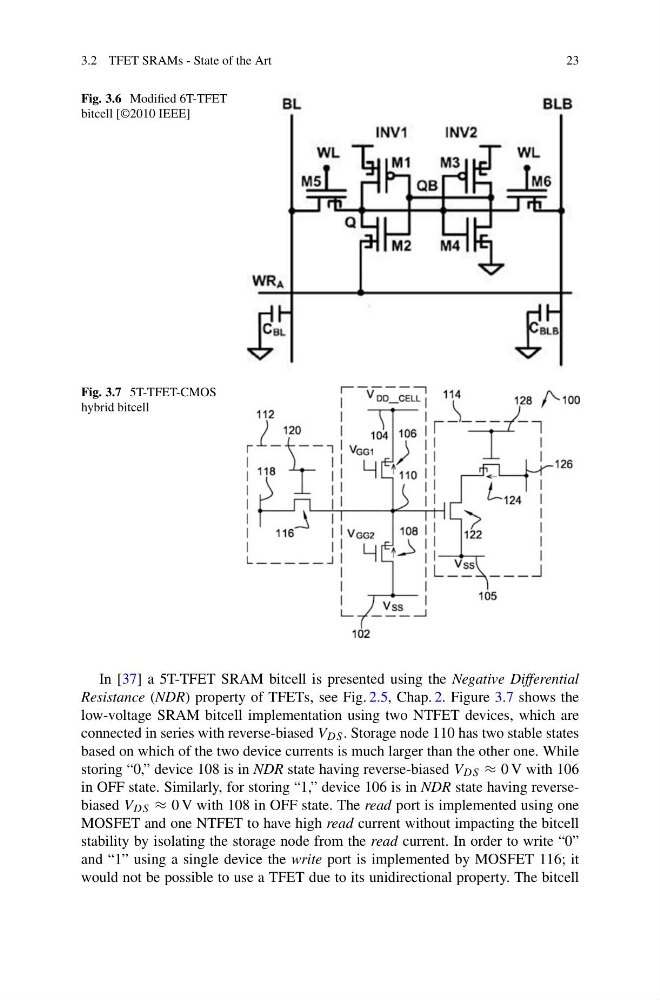
Fig. 3.6 Modified 6T-TFET
bitcell [©2010 IEEE]
Fig. 3.7 5T-TFET-CMOS
hybrid bitcell
In [37] a 5T-TFET SRAM bitcell is presented using the Negative Differential
Resistance (NDR) property of TFETs, see Fig. 2.5, Chap. 2. Figure 3.7 shows the
low-voltage SRAM bitcell implementation using two NTFET devices, which are
connected in series with reverse-biased V DS . Storage node 110 has two stable states
based on which of the two device currents is much larger than the other one. While
storing “0,” device 108 is in NDR state having reverse-biased V DS ≈ 0 V with 106
in OFF state. Similarly, for storing “1,” device 106 is in NDR state having reversebiased V DS ≈ 0 V with 108 in OFF state. The read port is implemented using one
MOSFET and one NTFET to have high read current without impacting the bitcell
stability by isolating the storage node from the read current. In order to write “0”
and “1” using a single device the write port is implemented by MOSFET 116; it
would not be possible to use a TFET due to its unidirectional property. The bitcell
23
Fig. 3.6 Modified 6T-TFET
bitcell [©2010 IEEE]
Fig. 3.7 5T-TFET-CMOS
hybrid bitcell
In [37] a 5T-TFET SRAM bitcell is presented using the Negative Differential
Resistance (NDR) property of TFETs, see Fig. 2.5, Chap. 2. Figure 3.7 shows the
low-voltage SRAM bitcell implementation using two NTFET devices, which are
connected in series with reverse-biased V DS . Storage node 110 has two stable states
based on which of the two device currents is much larger than the other one. While
storing “0,” device 108 is in NDR state having reverse-biased V DS ≈ 0 V with 106
in OFF state. Similarly, for storing “1,” device 106 is in NDR state having reversebiased V DS ≈ 0 V with 108 in OFF state. The read port is implemented using one
MOSFET and one NTFET to have high read current without impacting the bitcell
stability by isolating the storage node from the read current. In order to write “0”
and “1” using a single device the write port is implemented by MOSFET 116; it
would not be possible to use a TFET due to its unidirectional property. The bitcell