

3.2 TFET SRAMs - State of the Art
21
BLL (GND)
BLR (VDD)
WL
WL
VDD
GND
TR1
TR2
DR1
DR2
LD1
LD2
“1”
”0"
Ileak
WL
WL
VDD
GND
TR1
TR2
DR1
DR2
LD1
LD2
“1”
"0"
Iwrite
Ileak
WL
WL
VDD
GND
TR1
TR2
DR1
DR2
LD1
LD2
“1”
”0"
Ileak
BLL (GND)
BLR (VDD)
WL
WL
VDD
GND
TR1
TR2
DR1
DR2
LD1
LD2
“1”
”0"
Ileak
WL
WL
VDD
GND
TR1
TR2
DR1
DR2
LD1
LD2
“1”
"0"
Iwrite
Ileak
WL
WL
VDD
GND
TR1
TR2
DR1
DR2
LD1
LD2
“1”
”0"
Ileak
BLL (GND)
BLR (VDD)
WL
WL
VDD
GND
TR1
TR2
DR1
DR2
LD1
LD2
“1”
”0"
Ileak
WL
WL
VDD
GND
TR1
TR2
DR1
DR2
LD1
LD2
“1”
"0"
Iwrite
Ileak
WL
WL
VDD
GND
TR1
TR2
DR1
DR2
LD1
LD2
“1”
”0"
Ileak
WRITE
Word
Leakage
Leakage
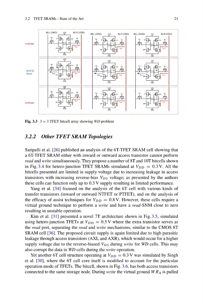
Fig. 3.3 3 × 3 TFET bitcell array showing WD problem
3.2.2 Other TFET SRAM Topologies
Saripalli et al. [26] published an analysis of the 6T-TFET SRAM cell showing that
a 6T-TFET SRAM either with inward or outward access transistor cannot perform
read and write simultaneously. They propose a number of 8T and 10T bitcells shown
in Fig. 3.4 for hetero-junction TFET SRAMs simulated at V DD = 0.3 V. All the
bitcells presented are limited in supply voltage due to increasing leakage in access
transistors with increasing reverse-bias V DS voltage; as presented by the authors
these cells can function only up to 0.3 V supply resulting in limited performance.
Yang et al. [34] focused on the analysis of the 6T cell with various kinds of
transfer transistors (inward or outward NTFET or PTFET), and on the analysis of
the efficacy of assist techniques for V DD = 0.8 V. However, these cells require a
virtual ground technique to perform a write and have a read-SNM close to zero
resulting in unstable operation.
Kim et al. [31] presented a novel 7T architecture shown in Fig. 3.5, simulated
using hetero-junction TFETs at V DD = 0.5 V where the extra transistor serves as
the read port, separating the read and write mechanisms, similar to the CMOS 8T
SRAM cell [36]. The proposed circuit supply is again limited due to high parasitic
leakage through access transistors (AXL and AXR), which would occur for a higher
supply voltage due to the reverse-biased V DS during write for WD cells. This may
also corrupt the data in WD cells during the write operation.
Yet another 6T cell structure operating at V DD = 0.3 V was simulated by Singh
et al. [30], where the 6T cell core itself is modified to account for the particular
operation mode of TFETs. The bitcell, shown in Fig. 3.6, has both access transistors
connected to the same storage node. During write the virtual ground W R A is pulled
21
BLL (GND)
BLR (VDD)
WL
WL
VDD
GND
TR1
TR2
DR1
DR2
LD1
LD2
“1”
”0"
Ileak
WL
WL
VDD
GND
TR1
TR2
DR1
DR2
LD1
LD2
“1”
"0"
Iwrite
Ileak
WL
WL
VDD
GND
TR1
TR2
DR1
DR2
LD1
LD2
“1”
”0"
Ileak
BLL (GND)
BLR (VDD)
WL
WL
VDD
GND
TR1
TR2
DR1
DR2
LD1
LD2
“1”
”0"
Ileak
WL
WL
VDD
GND
TR1
TR2
DR1
DR2
LD1
LD2
“1”
"0"
Iwrite
Ileak
WL
WL
VDD
GND
TR1
TR2
DR1
DR2
LD1
LD2
“1”
”0"
Ileak
BLL (GND)
BLR (VDD)
WL
WL
VDD
GND
TR1
TR2
DR1
DR2
LD1
LD2
“1”
”0"
Ileak
WL
WL
VDD
GND
TR1
TR2
DR1
DR2
LD1
LD2
“1”
"0"
Iwrite
Ileak
WL
WL
VDD
GND
TR1
TR2
DR1
DR2
LD1
LD2
“1”
”0"
Ileak
WRITE
Word
Leakage
Leakage
Fig. 3.3 3 × 3 TFET bitcell array showing WD problem
3.2.2 Other TFET SRAM Topologies
Saripalli et al. [26] published an analysis of the 6T-TFET SRAM cell showing that
a 6T-TFET SRAM either with inward or outward access transistor cannot perform
read and write simultaneously. They propose a number of 8T and 10T bitcells shown
in Fig. 3.4 for hetero-junction TFET SRAMs simulated at V DD = 0.3 V. All the
bitcells presented are limited in supply voltage due to increasing leakage in access
transistors with increasing reverse-bias V DS voltage; as presented by the authors
these cells can function only up to 0.3 V supply resulting in limited performance.
Yang et al. [34] focused on the analysis of the 6T cell with various kinds of
transfer transistors (inward or outward NTFET or PTFET), and on the analysis of
the efficacy of assist techniques for V DD = 0.8 V. However, these cells require a
virtual ground technique to perform a write and have a read-SNM close to zero
resulting in unstable operation.
Kim et al. [31] presented a novel 7T architecture shown in Fig. 3.5, simulated
using hetero-junction TFETs at V DD = 0.5 V where the extra transistor serves as
the read port, separating the read and write mechanisms, similar to the CMOS 8T
SRAM cell [36]. The proposed circuit supply is again limited due to high parasitic
leakage through access transistors (AXL and AXR), which would occur for a higher
supply voltage due to the reverse-biased V DS during write for WD cells. This may
also corrupt the data in WD cells during the write operation.
Yet another 6T cell structure operating at V DD = 0.3 V was simulated by Singh
et al. [30], where the 6T cell core itself is modified to account for the particular
operation mode of TFETs. The bitcell, shown in Fig. 3.6, has both access transistors
connected to the same storage node. During write the virtual ground W R A is pulled