

2.3 TFET Power and Delay Comparison with CMOS
15
N+
P+
NTFET
PTFET
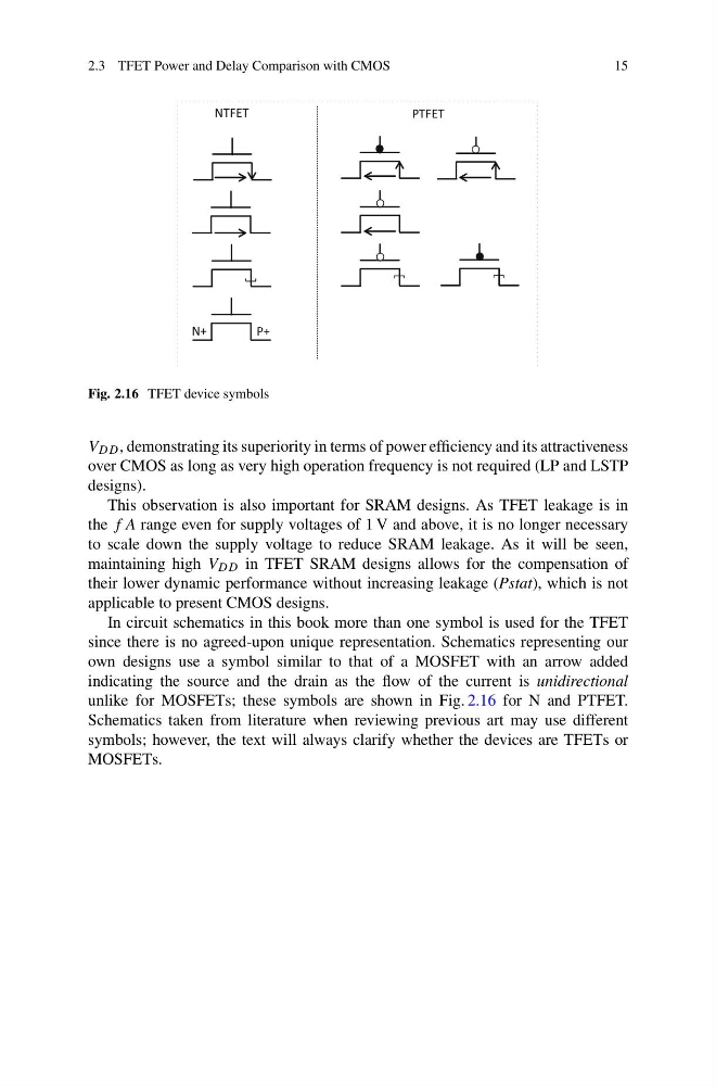
Fig. 2.16 TFET device symbols
V DD , demonstrating its superiority in terms of power efficiency and its attractiveness
over CMOS as long as very high operation frequency is not required (LP and LSTP
designs).
This observation is also important for SRAM designs. As TFET leakage is in
the f A range even for supply voltages of 1 V and above, it is no longer necessary
to scale down the supply voltage to reduce SRAM leakage. As it will be seen,
maintaining high V DD in TFET SRAM designs allows for the compensation of
their lower dynamic performance without increasing leakage (Pstat), which is not
applicable to present CMOS designs.
In circuit schematics in this book more than one symbol is used for the TFET
since there is no agreed-upon unique representation. Schematics representing our
own designs use a symbol similar to that of a MOSFET with an arrow added
indicating the source and the drain as the flow of the current is unidirectional
unlike for MOSFETs; these symbols are shown in Fig. 2.16 for N and PTFET.
Schematics taken from literature when reviewing previous art may use different
symbols; however, the text will always clarify whether the devices are TFETs or
MOSFETs.
15
N+
P+
NTFET
PTFET
Fig. 2.16 TFET device symbols
V DD , demonstrating its superiority in terms of power efficiency and its attractiveness
over CMOS as long as very high operation frequency is not required (LP and LSTP
designs).
This observation is also important for SRAM designs. As TFET leakage is in
the f A range even for supply voltages of 1 V and above, it is no longer necessary
to scale down the supply voltage to reduce SRAM leakage. As it will be seen,
maintaining high V DD in TFET SRAM designs allows for the compensation of
their lower dynamic performance without increasing leakage (Pstat), which is not
applicable to present CMOS designs.
In circuit schematics in this book more than one symbol is used for the TFET
since there is no agreed-upon unique representation. Schematics representing our
own designs use a symbol similar to that of a MOSFET with an arrow added
indicating the source and the drain as the flow of the current is unidirectional
unlike for MOSFETs; these symbols are shown in Fig. 2.16 for N and PTFET.
Schematics taken from literature when reviewing previous art may use different
symbols; however, the text will always clarify whether the devices are TFETs or
MOSFETs.