

12
2 State-of-the-Art TFET Devices
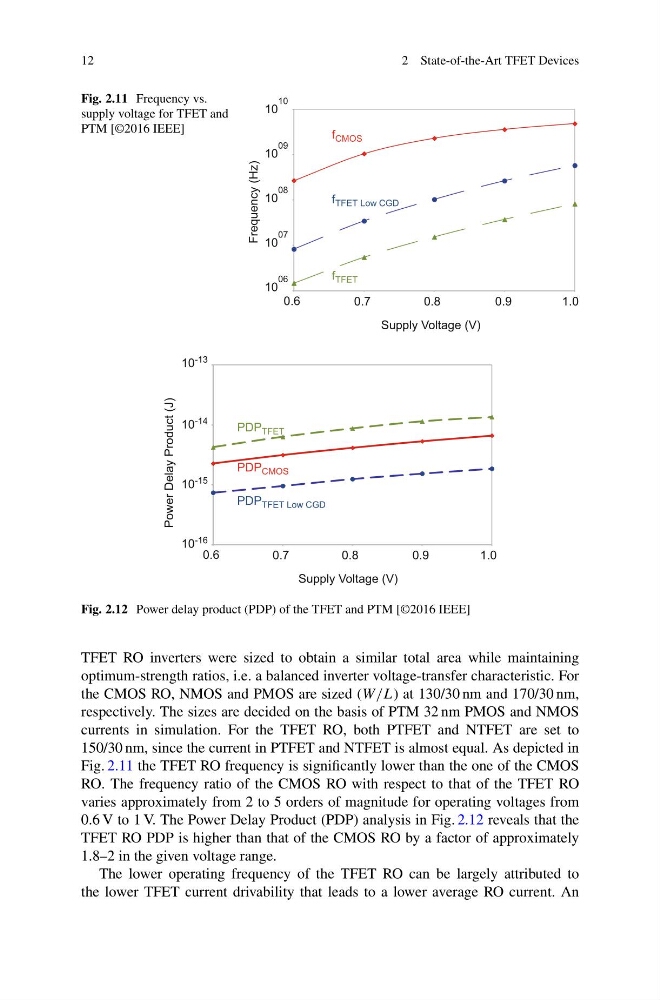
Fig. 2.11 Frequency vs.
supply voltage for TFET and
PTM [©2016 IEEE]
Supply Voltage (V)
Frequency (Hz)
0.6
0.7
0.8
0.9
1.0
f CMOS
f TFET
f TFET Low CGD
10
10
10
09
10
08
10
07
10
06
Supply Voltage (V)
Power Delay Product (J)
0.6
0.7
0.8
0.9
1.0
PDP CMOS
PDP TFET
PDP TFET Low CGD
10
-13
10
-14
10
-15
10
-16
Fig. 2.12 Power delay product (PDP) of the TFET and PTM [©2016 IEEE]
TFET RO inverters were sized to obtain a similar total area while maintaining
optimum-strength ratios, i.e. a balanced inverter voltage-transfer characteristic. For
the CMOS RO, NMOS and PMOS are sized (W/L) at 130/30 nm and 170/30 nm,
respectively. The sizes are decided on the basis of PTM 32 nm PMOS and NMOS
currents in simulation. For the TFET RO, both PTFET and NTFET are set to
150/30 nm, since the current in PTFET and NTFET is almost equal. As depicted in
Fig. 2.11 the TFET RO frequency is significantly lower than the one of the CMOS
RO. The frequency ratio of the CMOS RO with respect to that of the TFET RO
varies approximately from 2 to 5 orders of magnitude for operating voltages from
0.6 V to 1 V. The Power Delay Product (PDP) analysis in Fig. 2.12 reveals that the
TFET RO PDP is higher than that of the CMOS RO by a factor of approximately
1.8–2 in the given voltage range.
The lower operating frequency of the TFET RO can be largely attributed to
the lower TFET current drivability that leads to a lower average RO current. An
2 State-of-the-Art TFET Devices
Fig. 2.11 Frequency vs.
supply voltage for TFET and
PTM [©2016 IEEE]
Supply Voltage (V)
Frequency (Hz)
0.6
0.7
0.8
0.9
1.0
f CMOS
f TFET
f TFET Low CGD
10
10
10
09
10
08
10
07
10
06
Supply Voltage (V)
Power Delay Product (J)
0.6
0.7
0.8
0.9
1.0
PDP CMOS
PDP TFET
PDP TFET Low CGD
10
-13
10
-14
10
-15
10
-16
Fig. 2.12 Power delay product (PDP) of the TFET and PTM [©2016 IEEE]
TFET RO inverters were sized to obtain a similar total area while maintaining
optimum-strength ratios, i.e. a balanced inverter voltage-transfer characteristic. For
the CMOS RO, NMOS and PMOS are sized (W/L) at 130/30 nm and 170/30 nm,
respectively. The sizes are decided on the basis of PTM 32 nm PMOS and NMOS
currents in simulation. For the TFET RO, both PTFET and NTFET are set to
150/30 nm, since the current in PTFET and NTFET is almost equal. As depicted in
Fig. 2.11 the TFET RO frequency is significantly lower than the one of the CMOS
RO. The frequency ratio of the CMOS RO with respect to that of the TFET RO
varies approximately from 2 to 5 orders of magnitude for operating voltages from
0.6 V to 1 V. The Power Delay Product (PDP) analysis in Fig. 2.12 reveals that the
TFET RO PDP is higher than that of the CMOS RO by a factor of approximately
1.8–2 in the given voltage range.
The lower operating frequency of the TFET RO can be largely attributed to
the lower TFET current drivability that leads to a lower average RO current. An