

2.3 TFET Power and Delay Comparison with CMOS
11
V DS (V)
I
D (A/μm)
-0.25 V
10
-05
10
-07
10
-09
10
-11
10
-13
10
-15
10
-17
I
pTFET
Sims.
0
0.1
0.4
0.5
0.6
0.7
0.8
0.9
1.0
0.2
0.3
II
III
V GS = - 1V
Step +0.25V
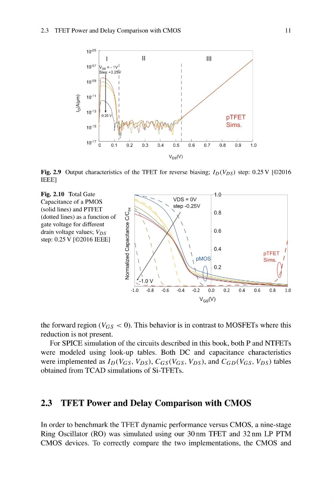
Fig. 2.9 Output characteristics of the TFET for reverse biasing; I D (V DS ) step: 0.25 V [©2016
IEEE]
Fig. 2.10 Total Gate
Capacitance of a PMOS
(solid lines) and PTFET
(dotted lines) as a function of
gate voltage for different
drain voltage values; V DS
step: 0.25 V [©2016 IEEE]
-1.0 -0.8 -0.6 -0.4 -0.2
0.0
0.2
0.4
0.6
0.8
1.0
V GS (V)
Normalized Capacitance C/C
ox
VDS = 0V
step -0.25V
pMOS
pTFET
Sims.
0.4
0.6
0.8
1.0
-1.0 V
0.2
the forward region (V GS < 0). This behavior is in contrast to MOSFETs where this
reduction is not present.
For SPICE simulation of the circuits described in this book, both P and NTFETs
were modeled using look-up tables. Both DC and capacitance characteristics
were implemented as I D (V GS , V DS ), C GS (V GS , V DS ), and C GD (V GS , V DS ) tables
obtained from TCAD simulations of Si-TFETs.
2.3 TFET Power and Delay Comparison with CMOS
In order to benchmark the TFET dynamic performance versus CMOS, a nine-stage
Ring Oscillator (RO) was simulated using our 30 nm TFET and 32 nm LP PTM
CMOS devices. To correctly compare the two implementations, the CMOS and
11
V DS (V)
I
D (A/μm)
-0.25 V
10
-05
10
-07
10
-09
10
-11
10
-13
10
-15
10
-17
I
pTFET
Sims.
0
0.1
0.4
0.5
0.6
0.7
0.8
0.9
1.0
0.2
0.3
II
III
V GS = - 1V
Step +0.25V
Fig. 2.9 Output characteristics of the TFET for reverse biasing; I D (V DS ) step: 0.25 V [©2016
IEEE]
Fig. 2.10 Total Gate
Capacitance of a PMOS
(solid lines) and PTFET
(dotted lines) as a function of
gate voltage for different
drain voltage values; V DS
step: 0.25 V [©2016 IEEE]
-1.0 -0.8 -0.6 -0.4 -0.2
0.0
0.2
0.4
0.6
0.8
1.0
V GS (V)
Normalized Capacitance C/C
ox
VDS = 0V
step -0.25V
pMOS
pTFET
Sims.
0.4
0.6
0.8
1.0
-1.0 V
0.2
the forward region (V GS < 0). This behavior is in contrast to MOSFETs where this
reduction is not present.
For SPICE simulation of the circuits described in this book, both P and NTFETs
were modeled using look-up tables. Both DC and capacitance characteristics
were implemented as I D (V GS , V DS ), C GS (V GS , V DS ), and C GD (V GS , V DS ) tables
obtained from TCAD simulations of Si-TFETs.
2.3 TFET Power and Delay Comparison with CMOS
In order to benchmark the TFET dynamic performance versus CMOS, a nine-stage
Ring Oscillator (RO) was simulated using our 30 nm TFET and 32 nm LP PTM
CMOS devices. To correctly compare the two implementations, the CMOS and