

2.2 Silicon TFET Device TCAD and SPICE Models
9
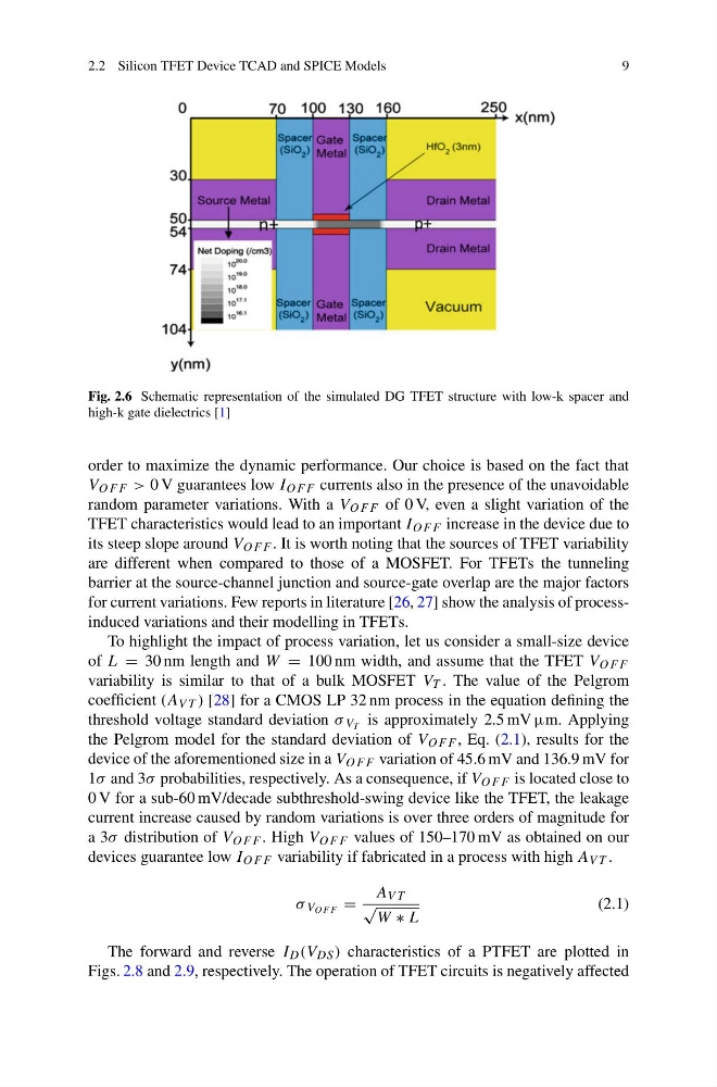
Fig. 2.6 Schematic representation of the simulated DG TFET structure with low-k spacer and
high-k gate dielectrics [1]
order to maximize the dynamic performance. Our choice is based on the fact that
V OF F > 0 V guarantees low I OF F currents also in the presence of the unavoidable
random parameter variations. With a V OF F of 0 V, even a slight variation of the
TFET characteristics would lead to an important I OF F increase in the device due to
its steep slope around V OF F . It is worth noting that the sources of TFET variability
are different when compared to those of a MOSFET. For TFETs the tunneling
barrier at the source-channel junction and source-gate overlap are the major factors
for current variations. Few reports in literature [26, 27] show the analysis of processinduced variations and their modelling in TFETs.
To highlight the impact of process variation, let us consider a small-size device
of L = 30 nm length and W = 100 nm width, and assume that the TFET V OF F
variability is similar to that of a bulk MOSFET V T . The value of the Pelgrom
coefficient (A V T ) [28] for a CMOS LP 32 nm process in the equation defining the
threshold voltage standard deviation σ V T is approximately 2.5 mV µm. Applying
the Pelgrom model for the standard deviation of V OF F , Eq. (2.1), results for the
device of the aforementioned size in a V OF F variation of 45.6 mV and 136.9 mV for
1σ and 3σ probabilities, respectively. As a consequence, if V OF F is located close to
0 V for a sub-60 mV/decade subthreshold-swing device like the TFET, the leakage
current increase caused by random variations is over three orders of magnitude for
a 3σ distribution of V OF F . High V OF F values of 150–170 mV as obtained on our
devices guarantee low I OF F variability if fabricated in a process with high A V T .
σ V OF F =
A V T
√
W ∗ L
(2.1)
The forward and reverse I D (V DS ) characteristics of a PTFET are plotted in
Figs. 2.8 and 2.9, respectively. The operation of TFET circuits is negatively affected
9
Fig. 2.6 Schematic representation of the simulated DG TFET structure with low-k spacer and
high-k gate dielectrics [1]
order to maximize the dynamic performance. Our choice is based on the fact that
V OF F > 0 V guarantees low I OF F currents also in the presence of the unavoidable
random parameter variations. With a V OF F of 0 V, even a slight variation of the
TFET characteristics would lead to an important I OF F increase in the device due to
its steep slope around V OF F . It is worth noting that the sources of TFET variability
are different when compared to those of a MOSFET. For TFETs the tunneling
barrier at the source-channel junction and source-gate overlap are the major factors
for current variations. Few reports in literature [26, 27] show the analysis of processinduced variations and their modelling in TFETs.
To highlight the impact of process variation, let us consider a small-size device
of L = 30 nm length and W = 100 nm width, and assume that the TFET V OF F
variability is similar to that of a bulk MOSFET V T . The value of the Pelgrom
coefficient (A V T ) [28] for a CMOS LP 32 nm process in the equation defining the
threshold voltage standard deviation σ V T is approximately 2.5 mV µm. Applying
the Pelgrom model for the standard deviation of V OF F , Eq. (2.1), results for the
device of the aforementioned size in a V OF F variation of 45.6 mV and 136.9 mV for
1σ and 3σ probabilities, respectively. As a consequence, if V OF F is located close to
0 V for a sub-60 mV/decade subthreshold-swing device like the TFET, the leakage
current increase caused by random variations is over three orders of magnitude for
a 3σ distribution of V OF F . High V OF F values of 150–170 mV as obtained on our
devices guarantee low I OF F variability if fabricated in a process with high A V T .
σ V OF F =
A V T
√
W ∗ L
(2.1)
The forward and reverse I D (V DS ) characteristics of a PTFET are plotted in
Figs. 2.8 and 2.9, respectively. The operation of TFET circuits is negatively affected