

8
2 State-of-the-Art TFET Devices
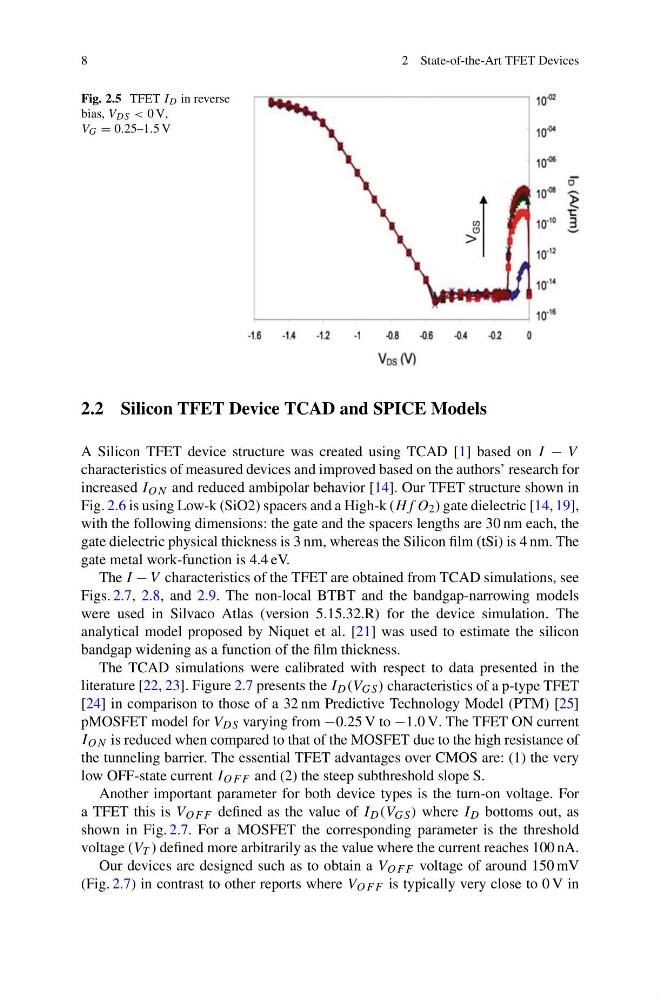
Fig. 2.5 TFET I D in reverse
bias, V DS < 0 V,
V G = 0.25–1.5 V
2.2 Silicon TFET Device TCAD and SPICE Models
A Silicon TFET device structure was created using TCAD [1] based on I − V
characteristics of measured devices and improved based on the authors’ research for
increased I ON and reduced ambipolar behavior [14]. Our TFET structure shown in
Fig. 2.6 is using Low-k (SiO2) spacers and a High-k (Hf O 2 ) gate dielectric [14, 19],
with the following dimensions: the gate and the spacers lengths are 30 nm each, the
gate dielectric physical thickness is 3 nm, whereas the Silicon film (tSi) is 4 nm. The
gate metal work-function is 4.4 eV.
The I − V characteristics of the TFET are obtained from TCAD simulations, see
Figs. 2.7, 2.8, and 2.9. The non-local BTBT and the bandgap-narrowing models
were used in Silvaco Atlas (version 5.15.32.R) for the device simulation. The
analytical model proposed by Niquet et al. [21] was used to estimate the silicon
bandgap widening as a function of the film thickness.
The TCAD simulations were calibrated with respect to data presented in the
literature [22, 23]. Figure 2.7 presents the I D (V GS ) characteristics of a p-type TFET
[24] in comparison to those of a 32 nm Predictive Technology Model (PTM) [25]
pMOSFET model for V DS varying from −0.25 V to −1.0 V. The TFET ON current
I ON is reduced when compared to that of the MOSFET due to the high resistance of
the tunneling barrier. The essential TFET advantages over CMOS are: (1) the very
low OFF-state current I OF F and (2) the steep subthreshold slope S.
Another important parameter for both device types is the turn-on voltage. For
a TFET this is V OF F defined as the value of I D (V GS ) where I D bottoms out, as
shown in Fig. 2.7. For a MOSFET the corresponding parameter is the threshold
voltage (V T ) defined more arbitrarily as the value where the current reaches 100 nA.
Our devices are designed such as to obtain a V OF F voltage of around 150 mV
(Fig. 2.7) in contrast to other reports where V OF F is typically very close to 0 V in
2 State-of-the-Art TFET Devices
Fig. 2.5 TFET I D in reverse
bias, V DS < 0 V,
V G = 0.25–1.5 V
2.2 Silicon TFET Device TCAD and SPICE Models
A Silicon TFET device structure was created using TCAD [1] based on I − V
characteristics of measured devices and improved based on the authors’ research for
increased I ON and reduced ambipolar behavior [14]. Our TFET structure shown in
Fig. 2.6 is using Low-k (SiO2) spacers and a High-k (Hf O 2 ) gate dielectric [14, 19],
with the following dimensions: the gate and the spacers lengths are 30 nm each, the
gate dielectric physical thickness is 3 nm, whereas the Silicon film (tSi) is 4 nm. The
gate metal work-function is 4.4 eV.
The I − V characteristics of the TFET are obtained from TCAD simulations, see
Figs. 2.7, 2.8, and 2.9. The non-local BTBT and the bandgap-narrowing models
were used in Silvaco Atlas (version 5.15.32.R) for the device simulation. The
analytical model proposed by Niquet et al. [21] was used to estimate the silicon
bandgap widening as a function of the film thickness.
The TCAD simulations were calibrated with respect to data presented in the
literature [22, 23]. Figure 2.7 presents the I D (V GS ) characteristics of a p-type TFET
[24] in comparison to those of a 32 nm Predictive Technology Model (PTM) [25]
pMOSFET model for V DS varying from −0.25 V to −1.0 V. The TFET ON current
I ON is reduced when compared to that of the MOSFET due to the high resistance of
the tunneling barrier. The essential TFET advantages over CMOS are: (1) the very
low OFF-state current I OF F and (2) the steep subthreshold slope S.
Another important parameter for both device types is the turn-on voltage. For
a TFET this is V OF F defined as the value of I D (V GS ) where I D bottoms out, as
shown in Fig. 2.7. For a MOSFET the corresponding parameter is the threshold
voltage (V T ) defined more arbitrarily as the value where the current reaches 100 nA.
Our devices are designed such as to obtain a V OF F voltage of around 150 mV
(Fig. 2.7) in contrast to other reports where V OF F is typically very close to 0 V in