

7.5 Adaptive Read Technique
119
Start of Read WL high
WL OFF, BL pre-charge ON,
SA output latched
BL
SP1
SP2
Q1
Q2
Q2b
Q1b
RdOk
RdNOk
BLB
Voltage [V]→
Voltage [V]→
Voltage [V]→
Voltage [V]→
Time[ns]→
Start of SA
→
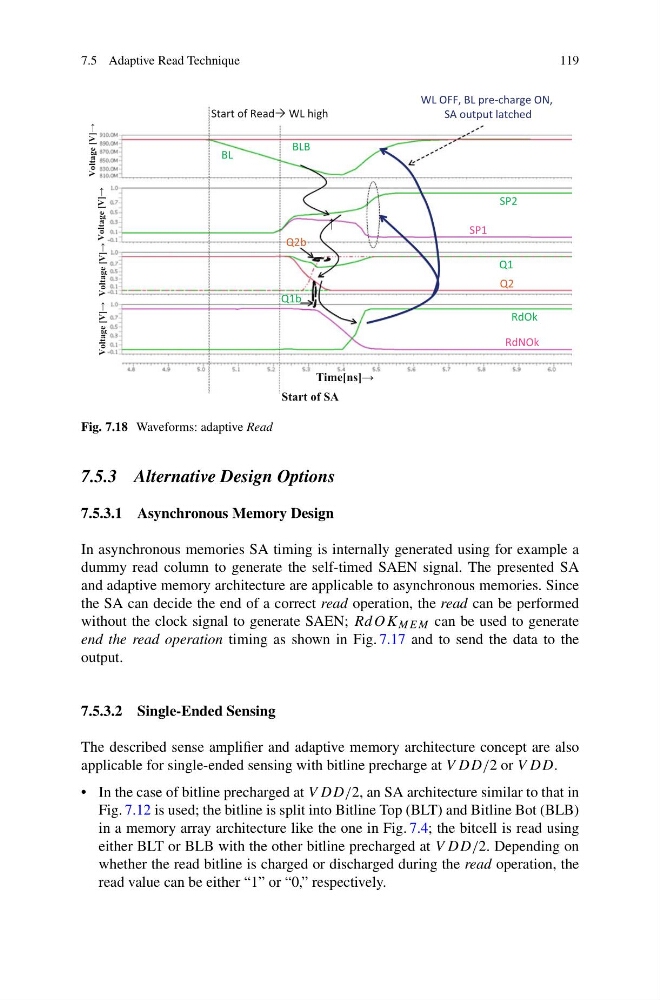
Fig. 7.18 Waveforms: adaptive Read
7.5.3 Alternative Design Options
7.5.3.1 Asynchronous Memory Design
In asynchronous memories SA timing is internally generated using for example a
dummy read column to generate the self-timed SAEN signal. The presented SA
and adaptive memory architecture are applicable to asynchronous memories. Since
the SA can decide the end of a correct read operation, the read can be performed
without the clock signal to generate SAEN; RdOK MEM can be used to generate
end the read operation timing as shown in Fig. 7.17 and to send the data to the
output.
7.5.3.2 Single-Ended Sensing
The described sense amplifier and adaptive memory architecture concept are also
applicable for single-ended sensing with bitline precharge at V DD/2 or V DD.
• In the case of bitline precharged at V DD/2, an SA architecture similar to that in
Fig. 7.12 is used; the bitline is split into Bitline Top (BLT) and Bitline Bot (BLB)
in a memory array architecture like the one in Fig. 7.4; the bitcell is read using
either BLT or BLB with the other bitline precharged at V DD/2. Depending on
whether the read bitline is charged or discharged during the read operation, the
read value can be either “1” or “0,” respectively.
119
Start of Read WL high
WL OFF, BL pre-charge ON,
SA output latched
BL
SP1
SP2
Q1
Q2
Q2b
Q1b
RdOk
RdNOk
BLB
Voltage [V]→
Voltage [V]→
Voltage [V]→
Voltage [V]→
Time[ns]→
Start of SA
→
Fig. 7.18 Waveforms: adaptive Read
7.5.3 Alternative Design Options
7.5.3.1 Asynchronous Memory Design
In asynchronous memories SA timing is internally generated using for example a
dummy read column to generate the self-timed SAEN signal. The presented SA
and adaptive memory architecture are applicable to asynchronous memories. Since
the SA can decide the end of a correct read operation, the read can be performed
without the clock signal to generate SAEN; RdOK MEM can be used to generate
end the read operation timing as shown in Fig. 7.17 and to send the data to the
output.
7.5.3.2 Single-Ended Sensing
The described sense amplifier and adaptive memory architecture concept are also
applicable for single-ended sensing with bitline precharge at V DD/2 or V DD.
• In the case of bitline precharged at V DD/2, an SA architecture similar to that in
Fig. 7.12 is used; the bitline is split into Bitline Top (BLT) and Bitline Bot (BLB)
in a memory array architecture like the one in Fig. 7.4; the bitcell is read using
either BLT or BLB with the other bitline precharged at V DD/2. Depending on
whether the read bitline is charged or discharged during the read operation, the
read value can be either “1” or “0,” respectively.