

118
7 Sensing Techniques
RdOK[0]
RdOK[1]
RdOK[n]
Address Decoder
WL Drivers
Pull-down WL’s@ROK
Bitcell Array
IO-Logic(Sense Amp. + Write logic)
Control logic
[Self-time tuning incase of unreliable read]
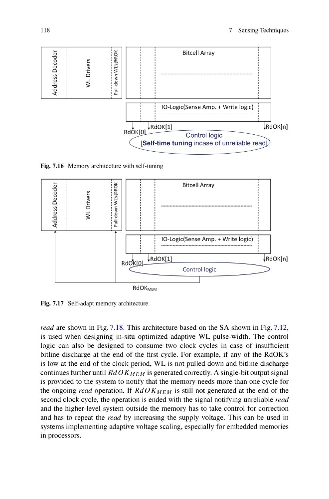
Fig. 7.16 Memory architecture with self-tuning
Control logic
RdOK[0]
RdOK[1]
RdOK[n]
Address Decoder
WL Drivers
Pull-down
WL’s@ROK
RdOK MEM
Bitcell Array
IO-Logic(Sense Amp. + Write logic)
Fig. 7.17 Self-adapt memory architecture
read are shown in Fig. 7.18. This architecture based on the SA shown in Fig. 7.12,
is used when designing in-situ optimized adaptive WL pulse-width. The control
logic can also be designed to consume two clock cycles in case of insufficient
bitline discharge at the end of the first cycle. For example, if any of the RdOK’s
is low at the end of the clock period, WL is not pulled down and bitline discharge
continues further until RdOK MEM is generated correctly. A single-bit output signal
is provided to the system to notify that the memory needs more than one cycle for
the ongoing read operation. If RdOK MEM is still not generated at the end of the
second clock cycle, the operation is ended with the signal notifying unreliable read
and the higher-level system outside the memory has to take control for correction
and has to repeat the read by increasing the supply voltage. This can be used in
systems implementing adaptive voltage scaling, especially for embedded memories
in processors.
7 Sensing Techniques
RdOK[0]
RdOK[1]
RdOK[n]
Address Decoder
WL Drivers
Pull-down WL’s@ROK
Bitcell Array
IO-Logic(Sense Amp. + Write logic)
Control logic
[Self-time tuning incase of unreliable read]
Fig. 7.16 Memory architecture with self-tuning
Control logic
RdOK[0]
RdOK[1]
RdOK[n]
Address Decoder
WL Drivers
Pull-down
WL’s@ROK
RdOK MEM
Bitcell Array
IO-Logic(Sense Amp. + Write logic)
Fig. 7.17 Self-adapt memory architecture
read are shown in Fig. 7.18. This architecture based on the SA shown in Fig. 7.12,
is used when designing in-situ optimized adaptive WL pulse-width. The control
logic can also be designed to consume two clock cycles in case of insufficient
bitline discharge at the end of the first cycle. For example, if any of the RdOK’s
is low at the end of the clock period, WL is not pulled down and bitline discharge
continues further until RdOK MEM is generated correctly. A single-bit output signal
is provided to the system to notify that the memory needs more than one cycle for
the ongoing read operation. If RdOK MEM is still not generated at the end of the
second clock cycle, the operation is ended with the signal notifying unreliable read
and the higher-level system outside the memory has to take control for correction
and has to repeat the read by increasing the supply voltage. This can be used in
systems implementing adaptive voltage scaling, especially for embedded memories
in processors.