

7.5 Adaptive Read Technique
113
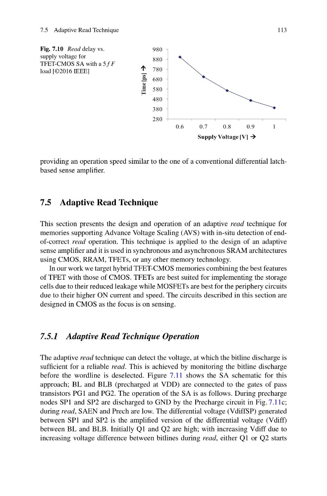
Fig. 7.10 Read delay vs.
supply voltage for
TFET-CMOS SA with a 5f F
load [©2016 IEEE]
280
380
480
580
680
780
880
980
0.6
0.7
0.8
0.9
1
Time [ps]
Supply Voltage [V]
providing an operation speed similar to the one of a conventional differential latchbased sense amplifier.
7.5 Adaptive Read Technique
This section presents the design and operation of an adaptive read technique for
memories supporting Advance Voltage Scaling (AVS) with in-situ detection of endof-correct read operation. This technique is applied to the design of an adaptive
sense amplifier and it is used in synchronous and asynchronous SRAM architectures
using CMOS, RRAM, TFETs, or any other memory technology.
In our work we target hybrid TFET-CMOS memories combining the best features
of TFET with those of CMOS. TFETs are best suited for implementing the storage
cells due to their reduced leakage while MOSFETs are best for the periphery circuits
due to their higher ON current and speed. The circuits described in this section are
designed in CMOS as the focus is on sensing.
7.5.1 Adaptive Read Technique Operation
The adaptive read technique can detect the voltage, at which the bitline discharge is
sufficient for a reliable read. This is achieved by monitoring the bitline discharge
before the wordline is deselected. Figure 7.11 shows the SA schematic for this
approach; BL and BLB (precharged at VDD) are connected to the gates of pass
transistors PG1 and PG2. The operation of the SA is as follows. During precharge
nodes SP1 and SP2 are discharged to GND by the Precharge circuit in Fig. 7.11c;
during read, SAEN and Prech are low. The differential voltage (VdiffSP) generated
between SP1 and SP2 is the amplified version of the differential voltage (Vdiff)
between BL and BLB. Initially Q1 and Q2 are high; with increasing Vdiff due to
increasing voltage difference between bitlines during read, either Q1 or Q2 starts
113
Fig. 7.10 Read delay vs.
supply voltage for
TFET-CMOS SA with a 5f F
load [©2016 IEEE]
280
380
480
580
680
780
880
980
0.6
0.7
0.8
0.9
1
Time [ps]
Supply Voltage [V]
providing an operation speed similar to the one of a conventional differential latchbased sense amplifier.
7.5 Adaptive Read Technique
This section presents the design and operation of an adaptive read technique for
memories supporting Advance Voltage Scaling (AVS) with in-situ detection of endof-correct read operation. This technique is applied to the design of an adaptive
sense amplifier and it is used in synchronous and asynchronous SRAM architectures
using CMOS, RRAM, TFETs, or any other memory technology.
In our work we target hybrid TFET-CMOS memories combining the best features
of TFET with those of CMOS. TFETs are best suited for implementing the storage
cells due to their reduced leakage while MOSFETs are best for the periphery circuits
due to their higher ON current and speed. The circuits described in this section are
designed in CMOS as the focus is on sensing.
7.5.1 Adaptive Read Technique Operation
The adaptive read technique can detect the voltage, at which the bitline discharge is
sufficient for a reliable read. This is achieved by monitoring the bitline discharge
before the wordline is deselected. Figure 7.11 shows the SA schematic for this
approach; BL and BLB (precharged at VDD) are connected to the gates of pass
transistors PG1 and PG2. The operation of the SA is as follows. During precharge
nodes SP1 and SP2 are discharged to GND by the Precharge circuit in Fig. 7.11c;
during read, SAEN and Prech are low. The differential voltage (VdiffSP) generated
between SP1 and SP2 is the amplified version of the differential voltage (Vdiff)
between BL and BLB. Initially Q1 and Q2 are high; with increasing Vdiff due to
increasing voltage difference between bitlines during read, either Q1 or Q2 starts