

112
7 Sensing Techniques
PRECH
BL
Q @different
sizing
Rdout
@different sizing
< 400 ps
1.1
0.9
0.7
0.5
0.3
0.1
-0.1
1.1
0.9
0.7
0.5
0.3
0.1
Voltage [v]→
Voltage [v]→
0.0 0.5 1.0 1.5 2.0
Time [ns]→
2.5 3.0 3.5 4.0 4.5
-0.1
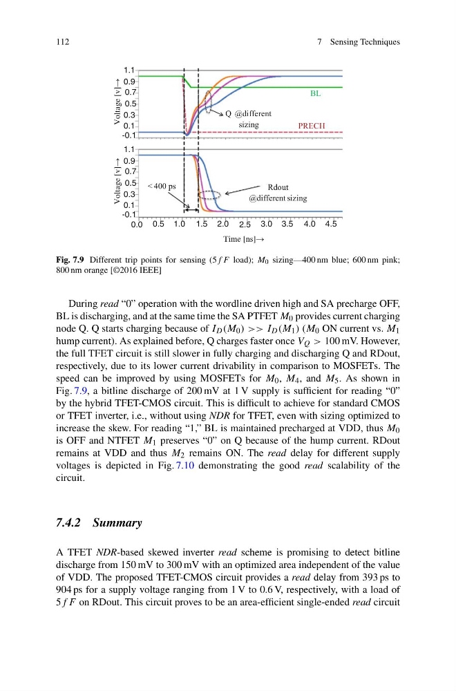
Fig. 7.9 Different trip points for sensing (5f F load); M 0 sizing—400 nm blue; 600 nm pink;
800 nm orange [©2016 IEEE]
During read “0” operation with the wordline driven high and SA precharge OFF,
BL is discharging, and at the same time the SA PTFET M 0 provides current charging
node Q. Q starts charging because of I D (M 0 ) >> I D (M 1 ) (M 0 ON current vs. M 1
hump current). As explained before, Q charges faster once V Q > 100 mV. However,
the full TFET circuit is still slower in fully charging and discharging Q and RDout,
respectively, due to its lower current drivability in comparison to MOSFETs. The
speed can be improved by using MOSFETs for M 0 , M 4 , and M 5 . As shown in
Fig. 7.9, a bitline discharge of 200 mV at 1 V supply is sufficient for reading “0”
by the hybrid TFET-CMOS circuit. This is difficult to achieve for standard CMOS
or TFET inverter, i.e., without using NDR for TFET, even with sizing optimized to
increase the skew. For reading “1,” BL is maintained precharged at VDD, thus M 0
is OFF and NTFET M 1 preserves “0” on Q because of the hump current. RDout
remains at VDD and thus M 2 remains ON. The read delay for different supply
voltages is depicted in Fig. 7.10 demonstrating the good read scalability of the
circuit.
7.4.2 Summary
A TFET NDR-based skewed inverter read scheme is promising to detect bitline
discharge from 150 mV to 300 mV with an optimized area independent of the value
of VDD. The proposed TFET-CMOS circuit provides a read delay from 393 ps to
904 ps for a supply voltage ranging from 1 V to 0.6 V, respectively, with a load of
5f F on RDout. This circuit proves to be an area-efficient single-ended read circuit
7 Sensing Techniques
PRECH
BL
Q @different
sizing
Rdout
@different sizing
< 400 ps
1.1
0.9
0.7
0.5
0.3
0.1
-0.1
1.1
0.9
0.7
0.5
0.3
0.1
Voltage [v]→
Voltage [v]→
0.0 0.5 1.0 1.5 2.0
Time [ns]→
2.5 3.0 3.5 4.0 4.5
-0.1
Fig. 7.9 Different trip points for sensing (5f F load); M 0 sizing—400 nm blue; 600 nm pink;
800 nm orange [©2016 IEEE]
During read “0” operation with the wordline driven high and SA precharge OFF,
BL is discharging, and at the same time the SA PTFET M 0 provides current charging
node Q. Q starts charging because of I D (M 0 ) >> I D (M 1 ) (M 0 ON current vs. M 1
hump current). As explained before, Q charges faster once V Q > 100 mV. However,
the full TFET circuit is still slower in fully charging and discharging Q and RDout,
respectively, due to its lower current drivability in comparison to MOSFETs. The
speed can be improved by using MOSFETs for M 0 , M 4 , and M 5 . As shown in
Fig. 7.9, a bitline discharge of 200 mV at 1 V supply is sufficient for reading “0”
by the hybrid TFET-CMOS circuit. This is difficult to achieve for standard CMOS
or TFET inverter, i.e., without using NDR for TFET, even with sizing optimized to
increase the skew. For reading “1,” BL is maintained precharged at VDD, thus M 0
is OFF and NTFET M 1 preserves “0” on Q because of the hump current. RDout
remains at VDD and thus M 2 remains ON. The read delay for different supply
voltages is depicted in Fig. 7.10 demonstrating the good read scalability of the
circuit.
7.4.2 Summary
A TFET NDR-based skewed inverter read scheme is promising to detect bitline
discharge from 150 mV to 300 mV with an optimized area independent of the value
of VDD. The proposed TFET-CMOS circuit provides a read delay from 393 ps to
904 ps for a supply voltage ranging from 1 V to 0.6 V, respectively, with a load of
5f F on RDout. This circuit proves to be an area-efficient single-ended read circuit