

7.4 TFET NDR Skewed Inverter-Based Sensing Method
111
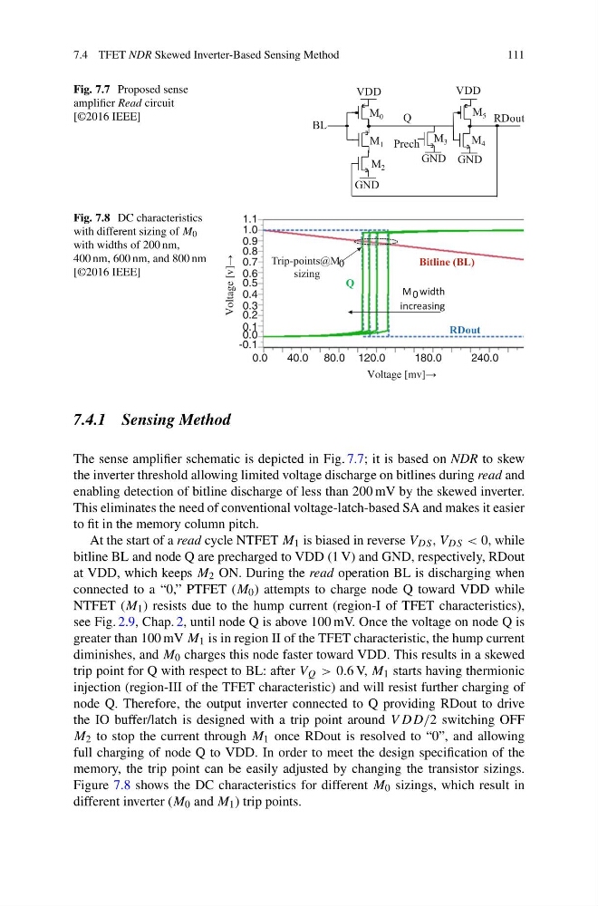
Fig. 7.7 Proposed sense
amplifier Read circuit
[©2016 IEEE]
VDD
GND
M 0
M 1
BL
VDD
GND
RDout
GND
Prech
Q
M 2
M 3
M 5
M 4
Fig. 7.8 DC characteristics
with different sizing of M 0
with widths of 200 nm,
400 nm, 600 nm, and 800 nm
[©2016 IEEE]
Bitline (BL)
RDout
Q
Trip-points@M 0
sizing
M 0 width
increasing
1.1
Voltage [v]→
Voltage [mv]→
1.0
0.9
0.8
0.7
0.6
0.5
0.4
0.3
0.2
0.1
0.0
0.0
40.0 80.0 120.0
180.0
240.0
-0.1
7.4.1 Sensing Method
The sense amplifier schematic is depicted in Fig. 7.7; it is based on NDR to skew
the inverter threshold allowing limited voltage discharge on bitlines during read and
enabling detection of bitline discharge of less than 200 mV by the skewed inverter.
This eliminates the need of conventional voltage-latch-based SA and makes it easier
to fit in the memory column pitch.
At the start of a read cycle NTFET M 1 is biased in reverse V DS , V DS < 0, while
bitline BL and node Q are precharged to VDD (1 V) and GND, respectively, RDout
at VDD, which keeps M 2 ON. During the read operation BL is discharging when
connected to a “0,” PTFET (M 0 ) attempts to charge node Q toward VDD while
NTFET (M 1 ) resists due to the hump current (region-I of TFET characteristics),
see Fig. 2.9, Chap. 2, until node Q is above 100 mV. Once the voltage on node Q is
greater than 100 mV M 1 is in region II of the TFET characteristic, the hump current
diminishes, and M 0 charges this node faster toward VDD. This results in a skewed
trip point for Q with respect to BL: after V Q > 0.6 V, M 1 starts having thermionic
injection (region-III of the TFET characteristic) and will resist further charging of
node Q. Therefore, the output inverter connected to Q providing RDout to drive
the IO buffer/latch is designed with a trip point around V DD/2 switching OFF
M 2 to stop the current through M 1 once RDout is resolved to “0”, and allowing
full charging of node Q to VDD. In order to meet the design specification of the
memory, the trip point can be easily adjusted by changing the transistor sizings.
Figure 7.8 shows the DC characteristics for different M 0 sizings, which result in
different inverter (M 0 and M 1 ) trip points.
111
Fig. 7.7 Proposed sense
amplifier Read circuit
[©2016 IEEE]
VDD
GND
M 0
M 1
BL
VDD
GND
RDout
GND
Prech
Q
M 2
M 3
M 5
M 4
Fig. 7.8 DC characteristics
with different sizing of M 0
with widths of 200 nm,
400 nm, 600 nm, and 800 nm
[©2016 IEEE]
Bitline (BL)
RDout
Q
Trip-points@M 0
sizing
M 0 width
increasing
1.1
Voltage [v]→
Voltage [mv]→
1.0
0.9
0.8
0.7
0.6
0.5
0.4
0.3
0.2
0.1
0.0
0.0
40.0 80.0 120.0
180.0
240.0
-0.1
7.4.1 Sensing Method
The sense amplifier schematic is depicted in Fig. 7.7; it is based on NDR to skew
the inverter threshold allowing limited voltage discharge on bitlines during read and
enabling detection of bitline discharge of less than 200 mV by the skewed inverter.
This eliminates the need of conventional voltage-latch-based SA and makes it easier
to fit in the memory column pitch.
At the start of a read cycle NTFET M 1 is biased in reverse V DS , V DS < 0, while
bitline BL and node Q are precharged to VDD (1 V) and GND, respectively, RDout
at VDD, which keeps M 2 ON. During the read operation BL is discharging when
connected to a “0,” PTFET (M 0 ) attempts to charge node Q toward VDD while
NTFET (M 1 ) resists due to the hump current (region-I of TFET characteristics),
see Fig. 2.9, Chap. 2, until node Q is above 100 mV. Once the voltage on node Q is
greater than 100 mV M 1 is in region II of the TFET characteristic, the hump current
diminishes, and M 0 charges this node faster toward VDD. This results in a skewed
trip point for Q with respect to BL: after V Q > 0.6 V, M 1 starts having thermionic
injection (region-III of the TFET characteristic) and will resist further charging of
node Q. Therefore, the output inverter connected to Q providing RDout to drive
the IO buffer/latch is designed with a trip point around V DD/2 switching OFF
M 2 to stop the current through M 1 once RDout is resolved to “0”, and allowing
full charging of node Q to VDD. In order to meet the design specification of the
memory, the trip point can be easily adjusted by changing the transistor sizings.
Figure 7.8 shows the DC characteristics for different M 0 sizings, which result in
different inverter (M 0 and M 1 ) trip points.