

110
7 Sensing Techniques
Voltage (V)
Time (ns)
Voltage (V)
Voltage (V)
Time (ns)
Voltage (V)
0.0
0.5
1.0
V(WL1[0])
V(BLR1_Top)
V(SAEN)
0.0
0.2
0.4
0.6
0.8
1.0
0.0
0.1
0.2
0.3
0.4
0.5
0.6
V(SA[62].Qb)
V(SA[62].Q)
V(RdOut1)
0.0
0.5
1.0
V(SAEN)
V(WL2[127])
V(BLR2_Bot)
0.0
0.2
0.4
0.6
0.8
1.0
0.0
0.1
0.2
0.3
0.4
0.5
0.6
V(SA[63].Q)
V(SA[63].Qb)
V(RdOut2)
a.
b.
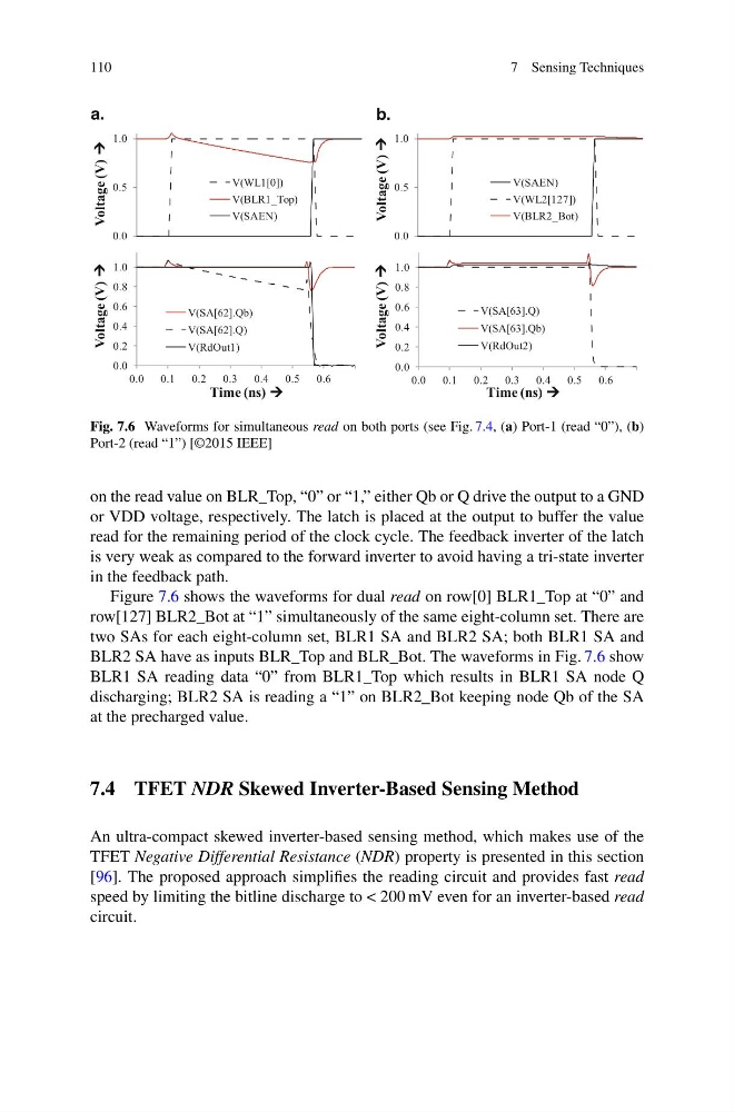
Fig. 7.6 Waveforms for simultaneous read on both ports (see Fig. 7.4, (a) Port-1 (read “0”), (b)
Port-2 (read “1”) [©2015 IEEE]
on the read value on BLR_Top, “0” or “1,” either Qb or Q drive the output to a GND
or VDD voltage, respectively. The latch is placed at the output to buffer the value
read for the remaining period of the clock cycle. The feedback inverter of the latch
is very weak as compared to the forward inverter to avoid having a tri-state inverter
in the feedback path.
Figure 7.6 shows the waveforms for dual read on row[0] BLR1_Top at “0” and
row[127] BLR2_Bot at “1” simultaneously of the same eight-column set. There are
two SAs for each eight-column set, BLR1 SA and BLR2 SA; both BLR1 SA and
BLR2 SA have as inputs BLR_Top and BLR_Bot. The waveforms in Fig. 7.6 show
BLR1 SA reading data “0” from BLR1_Top which results in BLR1 SA node Q
discharging; BLR2 SA is reading a “1” on BLR2_Bot keeping node Qb of the SA
at the precharged value.
7.4 TFET NDR Skewed Inverter-Based Sensing Method
An ultra-compact skewed inverter-based sensing method, which makes use of the
TFET Negative Differential Resistance (NDR) property is presented in this section
[96]. The proposed approach simplifies the reading circuit and provides fast read
speed by limiting the bitline discharge to < 200 mV even for an inverter-based read
circuit.
7 Sensing Techniques
Voltage (V)
Time (ns)
Voltage (V)
Voltage (V)
Time (ns)
Voltage (V)
0.0
0.5
1.0
V(WL1[0])
V(BLR1_Top)
V(SAEN)
0.0
0.2
0.4
0.6
0.8
1.0
0.0
0.1
0.2
0.3
0.4
0.5
0.6
V(SA[62].Qb)
V(SA[62].Q)
V(RdOut1)
0.0
0.5
1.0
V(SAEN)
V(WL2[127])
V(BLR2_Bot)
0.0
0.2
0.4
0.6
0.8
1.0
0.0
0.1
0.2
0.3
0.4
0.5
0.6
V(SA[63].Q)
V(SA[63].Qb)
V(RdOut2)
a.
b.
Fig. 7.6 Waveforms for simultaneous read on both ports (see Fig. 7.4, (a) Port-1 (read “0”), (b)
Port-2 (read “1”) [©2015 IEEE]
on the read value on BLR_Top, “0” or “1,” either Qb or Q drive the output to a GND
or VDD voltage, respectively. The latch is placed at the output to buffer the value
read for the remaining period of the clock cycle. The feedback inverter of the latch
is very weak as compared to the forward inverter to avoid having a tri-state inverter
in the feedback path.
Figure 7.6 shows the waveforms for dual read on row[0] BLR1_Top at “0” and
row[127] BLR2_Bot at “1” simultaneously of the same eight-column set. There are
two SAs for each eight-column set, BLR1 SA and BLR2 SA; both BLR1 SA and
BLR2 SA have as inputs BLR_Top and BLR_Bot. The waveforms in Fig. 7.6 show
BLR1 SA reading data “0” from BLR1_Top which results in BLR1 SA node Q
discharging; BLR2 SA is reading a “1” on BLR2_Bot keeping node Qb of the SA
at the precharged value.
7.4 TFET NDR Skewed Inverter-Based Sensing Method
An ultra-compact skewed inverter-based sensing method, which makes use of the
TFET Negative Differential Resistance (NDR) property is presented in this section
[96]. The proposed approach simplifies the reading circuit and provides fast read
speed by limiting the bitline discharge to < 200 mV even for an inverter-based read
circuit.