

6.5 Ultra-Low-Power TFET Ternary CAM (TCAM)
103
Cell and Array
Cell Area
0.293 μm 2
Size-Array
16Kb (128x128)
Dimension 82.71x58.06 μm 2
Array Area 4802.14 μm 2
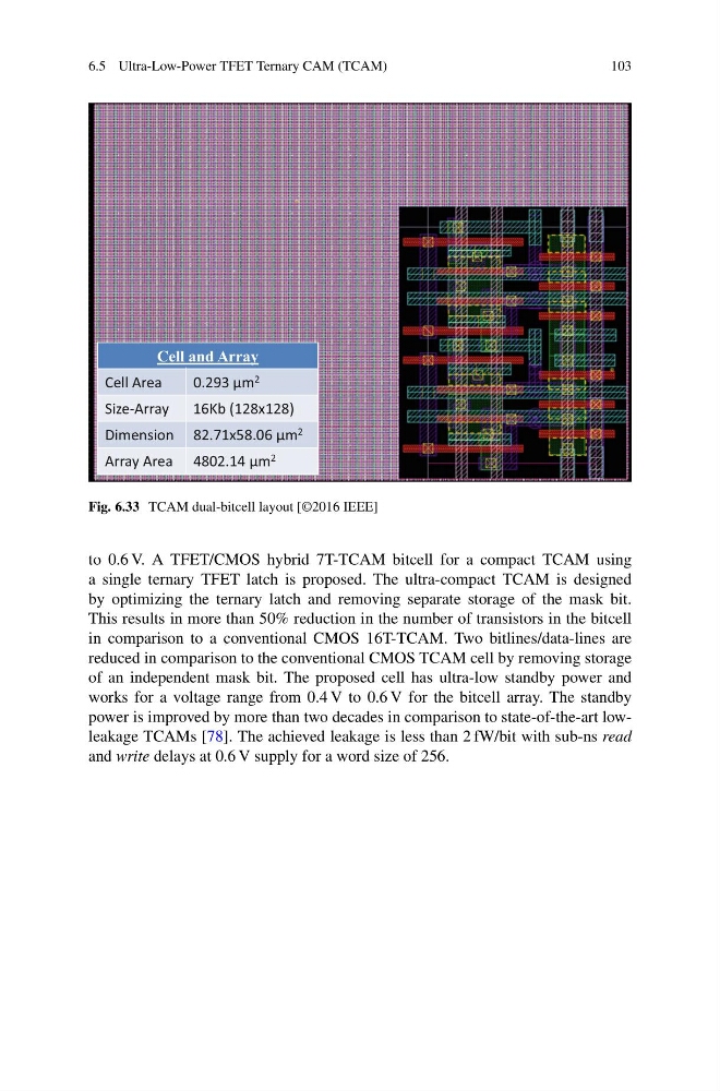
Fig. 6.33 TCAM dual-bitcell layout [©2016 IEEE]
to 0.6 V. A TFET/CMOS hybrid 7T-TCAM bitcell for a compact TCAM using
a single ternary TFET latch is proposed. The ultra-compact TCAM is designed
by optimizing the ternary latch and removing separate storage of the mask bit.
This results in more than 50% reduction in the number of transistors in the bitcell
in comparison to a conventional CMOS 16T-TCAM. Two bitlines/data-lines are
reduced in comparison to the conventional CMOS TCAM cell by removing storage
of an independent mask bit. The proposed cell has ultra-low standby power and
works for a voltage range from 0.4 V to 0.6 V for the bitcell array. The standby
power is improved by more than two decades in comparison to state-of-the-art lowleakage TCAMs [78]. The achieved leakage is less than 2 fW/bit with sub-ns read
and write delays at 0.6 V supply for a word size of 256.
103
Cell and Array
Cell Area
0.293 μm 2
Size-Array
16Kb (128x128)
Dimension 82.71x58.06 μm 2
Array Area 4802.14 μm 2
Fig. 6.33 TCAM dual-bitcell layout [©2016 IEEE]
to 0.6 V. A TFET/CMOS hybrid 7T-TCAM bitcell for a compact TCAM using
a single ternary TFET latch is proposed. The ultra-compact TCAM is designed
by optimizing the ternary latch and removing separate storage of the mask bit.
This results in more than 50% reduction in the number of transistors in the bitcell
in comparison to a conventional CMOS 16T-TCAM. Two bitlines/data-lines are
reduced in comparison to the conventional CMOS TCAM cell by removing storage
of an independent mask bit. The proposed cell has ultra-low standby power and
works for a voltage range from 0.4 V to 0.6 V for the bitcell array. The standby
power is improved by more than two decades in comparison to state-of-the-art lowleakage TCAMs [78]. The achieved leakage is less than 2 fW/bit with sub-ns read
and write delays at 0.6 V supply for a word size of 256.