

6.5 Ultra-Low-Power TFET Ternary CAM (TCAM)
101
VDD
GND
M 0
M 1
VDD
GND
Q0
M 2
GND
ML
DL
DLB
Q1
DLB
DL
WWL
WWL
M 3
M 4
M 5
M 6
M 0 to M 4 TFETs
M 5 , M 6 MOSFETs
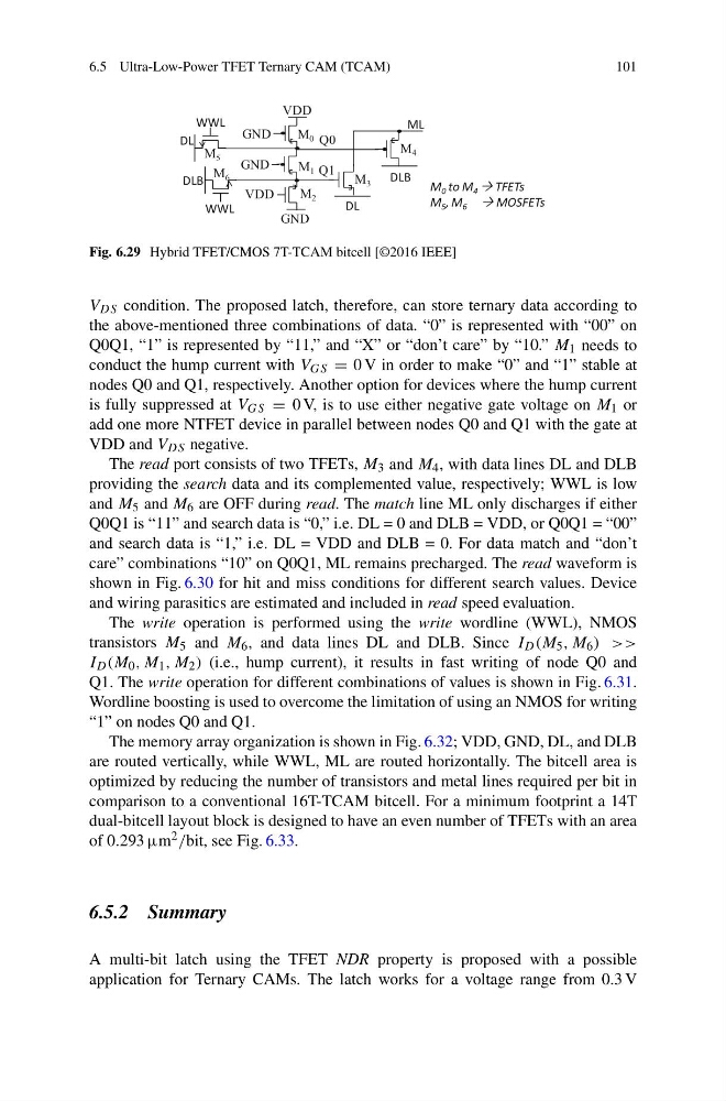
Fig. 6.29 Hybrid TFET/CMOS 7T-TCAM bitcell [©2016 IEEE]
V DS condition. The proposed latch, therefore, can store ternary data according to
the above-mentioned three combinations of data. “0” is represented with “00” on
Q0Q1, “1” is represented by “11,” and “X” or “don’t care” by “10.” M 1 needs to
conduct the hump current with V GS = 0 V in order to make “0” and “1” stable at
nodes Q0 and Q1, respectively. Another option for devices where the hump current
is fully suppressed at V GS = 0 V, is to use either negative gate voltage on M 1 or
add one more NTFET device in parallel between nodes Q0 and Q1 with the gate at
VDD and V DS negative.
The read port consists of two TFETs, M 3 and M 4 , with data lines DL and DLB
providing the search data and its complemented value, respectively; WWL is low
and M 5 and M 6 are OFF during read. The match line ML only discharges if either
Q0Q1 is “11” and search data is “0,” i.e. DL = 0 and DLB = VDD, or Q0Q1 = “00”
and search data is “1,” i.e. DL = VDD and DLB = 0. For data match and “don’t
care” combinations “10” on Q0Q1, ML remains precharged. The read waveform is
shown in Fig. 6.30 for hit and miss conditions for different search values. Device
and wiring parasitics are estimated and included in read speed evaluation.
The write operation is performed using the write wordline (WWL), NMOS
transistors M 5 and M 6 , and data lines DL and DLB. Since I D (M 5 , M 6 ) >>
I D (M 0 , M 1 , M 2 ) (i.e., hump current), it results in fast writing of node Q0 and
Q1. The write operation for different combinations of values is shown in Fig. 6.31.
Wordline boosting is used to overcome the limitation of using an NMOS for writing
“1” on nodes Q0 and Q1.
The memory array organization is shown in Fig. 6.32; VDD, GND, DL, and DLB
are routed vertically, while WWL, ML are routed horizontally. The bitcell area is
optimized by reducing the number of transistors and metal lines required per bit in
comparison to a conventional 16T-TCAM bitcell. For a minimum footprint a 14T
dual-bitcell layout block is designed to have an even number of TFETs with an area
of 0.293 µm 2 /bit, see Fig. 6.33.
6.5.2 Summary
A multi-bit latch using the TFET NDR property is proposed with a possible
application for Ternary CAMs. The latch works for a voltage range from 0.3 V
101
VDD
GND
M 0
M 1
VDD
GND
Q0
M 2
GND
ML
DL
DLB
Q1
DLB
DL
WWL
WWL
M 3
M 4
M 5
M 6
M 0 to M 4 TFETs
M 5 , M 6 MOSFETs
Fig. 6.29 Hybrid TFET/CMOS 7T-TCAM bitcell [©2016 IEEE]
V DS condition. The proposed latch, therefore, can store ternary data according to
the above-mentioned three combinations of data. “0” is represented with “00” on
Q0Q1, “1” is represented by “11,” and “X” or “don’t care” by “10.” M 1 needs to
conduct the hump current with V GS = 0 V in order to make “0” and “1” stable at
nodes Q0 and Q1, respectively. Another option for devices where the hump current
is fully suppressed at V GS = 0 V, is to use either negative gate voltage on M 1 or
add one more NTFET device in parallel between nodes Q0 and Q1 with the gate at
VDD and V DS negative.
The read port consists of two TFETs, M 3 and M 4 , with data lines DL and DLB
providing the search data and its complemented value, respectively; WWL is low
and M 5 and M 6 are OFF during read. The match line ML only discharges if either
Q0Q1 is “11” and search data is “0,” i.e. DL = 0 and DLB = VDD, or Q0Q1 = “00”
and search data is “1,” i.e. DL = VDD and DLB = 0. For data match and “don’t
care” combinations “10” on Q0Q1, ML remains precharged. The read waveform is
shown in Fig. 6.30 for hit and miss conditions for different search values. Device
and wiring parasitics are estimated and included in read speed evaluation.
The write operation is performed using the write wordline (WWL), NMOS
transistors M 5 and M 6 , and data lines DL and DLB. Since I D (M 5 , M 6 ) >>
I D (M 0 , M 1 , M 2 ) (i.e., hump current), it results in fast writing of node Q0 and
Q1. The write operation for different combinations of values is shown in Fig. 6.31.
Wordline boosting is used to overcome the limitation of using an NMOS for writing
“1” on nodes Q0 and Q1.
The memory array organization is shown in Fig. 6.32; VDD, GND, DL, and DLB
are routed vertically, while WWL, ML are routed horizontally. The bitcell area is
optimized by reducing the number of transistors and metal lines required per bit in
comparison to a conventional 16T-TCAM bitcell. For a minimum footprint a 14T
dual-bitcell layout block is designed to have an even number of TFETs with an area
of 0.293 µm 2 /bit, see Fig. 6.33.
6.5.2 Summary
A multi-bit latch using the TFET NDR property is proposed with a possible
application for Ternary CAMs. The latch works for a voltage range from 0.3 V