

100
6 Content-Addressable Memories
8Kb-TestMacro (2222.22μm x 150μm)
WL logic & Drivers
Test-Logic
IO-Logic
Array
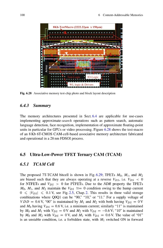
Fig. 6.28 Associative memory test-chip photo and block layout description
6.4.3 Summary
The memory architectures presented in Sect. 6.4 are applicable for use-cases
implementing approximate-search operations such as pattern search, automatic
language detection, face recognition, implementation of approximate floating-point
units in particular for GPUs or video processing. Figure 6.28 shows the test-macro
of an 8 Kb 6T-CMOS CAM-cell-based associative memory architecture fabricated
and operational in a 28 nm FDSOI process.
6.5 Ultra-Low-Power TFET Ternary CAM (TCAM)
6.5.1 TCAM Cell
The proposed 7T-TCAM bitcell is shown in Fig. 6.29; TFETs M 0 , M 1 , and M 2
are biased such that they are always operating at a reverse V DS , i.e. V DS < 0
for NTFETs and V DS > 0 for PTFETs. Due to the NDR property the TFETs
M 0 , M 1 , and M 2 maintain the V DS = 0 condition owing to the hump current
0 |V DS | 0.1 V, see Fig. 2.5, Chap. 2. This results in three valid storage
combinations where Q0Q1 can be “00,” “10,” or “11.” For a supply voltage of
V DD = 0.6 V, “00” is maintained by M 1 and M 2 with both having V DS = 0 V
and M 0 having V DS = 0.6 V, i.e. a minimum current; similarly “11” is maintained
by M 0 and M 1 with V DS = 0 V and M 2 with V DS = −0.6 V; “10” is maintained
by M 0 and M 2 with V DS = 0 V, and M 1 with V DS = 0.6 V. The value of “01”
is an unstable condition, i.e. a forbidden state, with M 1 switched ON in forward
6 Content-Addressable Memories
8Kb-TestMacro (2222.22μm x 150μm)
WL logic & Drivers
Test-Logic
IO-Logic
Array
Fig. 6.28 Associative memory test-chip photo and block layout description
6.4.3 Summary
The memory architectures presented in Sect. 6.4 are applicable for use-cases
implementing approximate-search operations such as pattern search, automatic
language detection, face recognition, implementation of approximate floating-point
units in particular for GPUs or video processing. Figure 6.28 shows the test-macro
of an 8 Kb 6T-CMOS CAM-cell-based associative memory architecture fabricated
and operational in a 28 nm FDSOI process.
6.5 Ultra-Low-Power TFET Ternary CAM (TCAM)
6.5.1 TCAM Cell
The proposed 7T-TCAM bitcell is shown in Fig. 6.29; TFETs M 0 , M 1 , and M 2
are biased such that they are always operating at a reverse V DS , i.e. V DS < 0
for NTFETs and V DS > 0 for PTFETs. Due to the NDR property the TFETs
M 0 , M 1 , and M 2 maintain the V DS = 0 condition owing to the hump current
0 |V DS | 0.1 V, see Fig. 2.5, Chap. 2. This results in three valid storage
combinations where Q0Q1 can be “00,” “10,” or “11.” For a supply voltage of
V DD = 0.6 V, “00” is maintained by M 1 and M 2 with both having V DS = 0 V
and M 0 having V DS = 0.6 V, i.e. a minimum current; similarly “11” is maintained
by M 0 and M 1 with V DS = 0 V and M 2 with V DS = −0.6 V; “10” is maintained
by M 0 and M 2 with V DS = 0 V, and M 1 with V DS = 0.6 V. The value of “01”
is an unstable condition, i.e. a forbidden state, with M 1 switched ON in forward