

6.4 Associative Memory Architecture
95
Table 6.6 Voltages during
write for selected and HS
cells (writing “1”)
Column written
(active cells)
Other columns
(HS cells)
BL
0 V
0.5 V
WL1 1 V
1 V
WL2 0 V
0 V
VDD 1 V
1 V
Time [μs]
CLK
CLK_Int
BL[0]
WL1[0]
WL2[0]
Q[0]
QR[0]
CLK
CLK_Int
BL[0]
WL1[0]
WL2[1]
Q[0]
QR[0]
1.1
0.7
0.3
0.1
1.1
Voltage [V] Voltage [V]
Voltage [V]
Voltage [V]
0.7
0.3
0.1
1.1
0.7
0.3
0.1
1.1
0.7
0.3
-0.1
1.1
0.7
0.3
-0.1
1.1
0.7
0.3
-0.1
1.1
0.8
0.5
0.2
0.1
1.299
1.301
1.303
1.305
0.1
0.2
0.5
0.8
1.1
1.30002 1.30006
1.30010 1.30014 1.30018
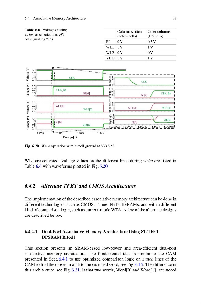
Fig. 6.20 Write operation with bitcell ground at V DD/2
WLs are activated. Voltage values on the different lines during write are listed in
Table 6.6 with waveforms plotted in Fig. 6.20.
6.4.2 Alternate TFET and CMOS Architectures
The implementation of the described associative memory architecture can be done in
different technologies, such as CMOS, Tunnel FETs, ReRAMs, and with a different
kind of comparison logic, such as current-mode WTA. A few of the alternate designs
are described below.
6.4.2.1 Dual-Port Associative Memory Architecture Using 8T-TFET
DPSRAM Bitcell
This section presents an SRAM-based low-power and area-efficient dual-port
associative memory architecture. The fundamental idea is similar to the CAM
presented in Sect. 6.4.1 to use optimized comparison logic on match lines of the
CAM to find the closest match to the searched word, see Fig. 6.15. The difference in
this architecture, see Fig. 6.21, is that two words, Word[0] and Word[1], are stored
95
Table 6.6 Voltages during
write for selected and HS
cells (writing “1”)
Column written
(active cells)
Other columns
(HS cells)
BL
0 V
0.5 V
WL1 1 V
1 V
WL2 0 V
0 V
VDD 1 V
1 V
Time [μs]
CLK
CLK_Int
BL[0]
WL1[0]
WL2[0]
Q[0]
QR[0]
CLK
CLK_Int
BL[0]
WL1[0]
WL2[1]
Q[0]
QR[0]
1.1
0.7
0.3
0.1
1.1
Voltage [V] Voltage [V]
Voltage [V]
Voltage [V]
0.7
0.3
0.1
1.1
0.7
0.3
0.1
1.1
0.7
0.3
-0.1
1.1
0.7
0.3
-0.1
1.1
0.7
0.3
-0.1
1.1
0.8
0.5
0.2
0.1
1.299
1.301
1.303
1.305
0.1
0.2
0.5
0.8
1.1
1.30002 1.30006
1.30010 1.30014 1.30018
Fig. 6.20 Write operation with bitcell ground at V DD/2
WLs are activated. Voltage values on the different lines during write are listed in
Table 6.6 with waveforms plotted in Fig. 6.20.
6.4.2 Alternate TFET and CMOS Architectures
The implementation of the described associative memory architecture can be done in
different technologies, such as CMOS, Tunnel FETs, ReRAMs, and with a different
kind of comparison logic, such as current-mode WTA. A few of the alternate designs
are described below.
6.4.2.1 Dual-Port Associative Memory Architecture Using 8T-TFET
DPSRAM Bitcell
This section presents an SRAM-based low-power and area-efficient dual-port
associative memory architecture. The fundamental idea is similar to the CAM
presented in Sect. 6.4.1 to use optimized comparison logic on match lines of the
CAM to find the closest match to the searched word, see Fig. 6.15. The difference in
this architecture, see Fig. 6.21, is that two words, Word[0] and Word[1], are stored