

38
2 Fundamental Properties of Mem-Elements
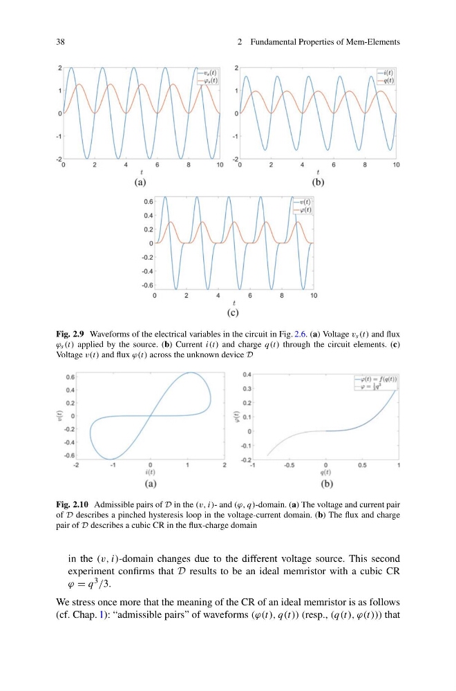
Fig. 2.9 Waveforms of the electrical variables in the circuit in Fig. 2.6. (a) Voltage v s (t) and flux
ϕ s (t) applied by the source. (b) Current i(t) and charge q(t) through the circuit elements. (c)
Voltage v(t) and flux ϕ(t) across the unknown device D
Fig. 2.10 Admissible pairs of D in the (v, i)- and (ϕ, q)-domain. (a) The voltage and current pair
of D describes a pinched hysteresis loop in the voltage-current domain. (b) The flux and charge
pair of D describes a cubic CR in the flux-charge domain
in the (v, i)-domain changes due to the different voltage source. This second
experiment confirms that D results to be an ideal memristor with a cubic CR
ϕ = q 3 /3.
We stress once more that the meaning of the CR of an ideal memristor is as follows
(cf. Chap. 1): “admissible pairs” of waveforms (ϕ(t), q(t)) (resp., (q(t), ϕ(t))) that
2 Fundamental Properties of Mem-Elements
Fig. 2.9 Waveforms of the electrical variables in the circuit in Fig. 2.6. (a) Voltage v s (t) and flux
ϕ s (t) applied by the source. (b) Current i(t) and charge q(t) through the circuit elements. (c)
Voltage v(t) and flux ϕ(t) across the unknown device D
Fig. 2.10 Admissible pairs of D in the (v, i)- and (ϕ, q)-domain. (a) The voltage and current pair
of D describes a pinched hysteresis loop in the voltage-current domain. (b) The flux and charge
pair of D describes a cubic CR in the flux-charge domain
in the (v, i)-domain changes due to the different voltage source. This second
experiment confirms that D results to be an ideal memristor with a cubic CR
ϕ = q 3 /3.
We stress once more that the meaning of the CR of an ideal memristor is as follows
(cf. Chap. 1): “admissible pairs” of waveforms (ϕ(t), q(t)) (resp., (q(t), ϕ(t))) that