

2.1 Ideal Memristor: Basic Properties and Signatures
37
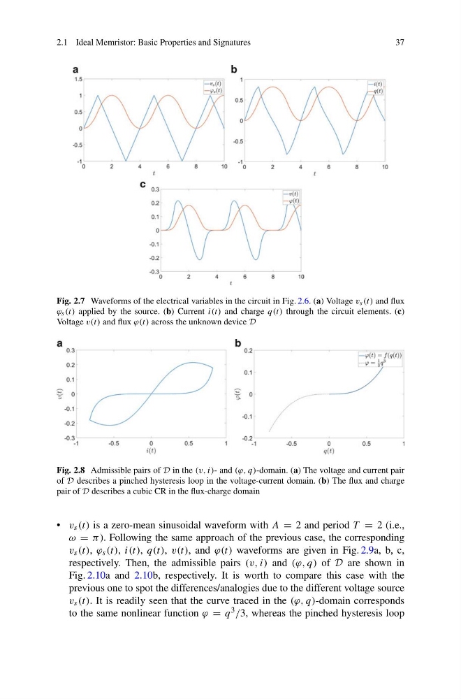
Fig. 2.7 Waveforms of the electrical variables in the circuit in Fig. 2.6. (a) Voltage v s (t) and flux
ϕ s (t) applied by the source. (b) Current i(t) and charge q(t) through the circuit elements. (c)
Voltage v(t) and flux ϕ(t) across the unknown device D
Fig. 2.8 Admissible pairs of D in the (v, i)- and (ϕ, q)-domain. (a) The voltage and current pair
of D describes a pinched hysteresis loop in the voltage-current domain. (b) The flux and charge
pair of D describes a cubic CR in the flux-charge domain
• v s (t) is a zero-mean sinusoidal waveform with A = 2 and period T = 2 (i.e.,
ω = π ). Following the same approach of the previous case, the corresponding
v s (t), ϕ s (t), i(t), q(t), v(t), and ϕ(t) waveforms are given in Fig. 2.9a, b, c,
respectively. Then, the admissible pairs (v, i) and (ϕ, q) of D are shown in
Fig. 2.10a and 2.10b, respectively. It is worth to compare this case with the
previous one to spot the differences/analogies due to the different voltage source
v s (t). It is readily seen that the curve traced in the (ϕ, q)-domain corresponds
to the same nonlinear function ϕ = q 3 /3, whereas the pinched hysteresis loop
37
Fig. 2.7 Waveforms of the electrical variables in the circuit in Fig. 2.6. (a) Voltage v s (t) and flux
ϕ s (t) applied by the source. (b) Current i(t) and charge q(t) through the circuit elements. (c)
Voltage v(t) and flux ϕ(t) across the unknown device D
Fig. 2.8 Admissible pairs of D in the (v, i)- and (ϕ, q)-domain. (a) The voltage and current pair
of D describes a pinched hysteresis loop in the voltage-current domain. (b) The flux and charge
pair of D describes a cubic CR in the flux-charge domain
• v s (t) is a zero-mean sinusoidal waveform with A = 2 and period T = 2 (i.e.,
ω = π ). Following the same approach of the previous case, the corresponding
v s (t), ϕ s (t), i(t), q(t), v(t), and ϕ(t) waveforms are given in Fig. 2.9a, b, c,
respectively. Then, the admissible pairs (v, i) and (ϕ, q) of D are shown in
Fig. 2.10a and 2.10b, respectively. It is worth to compare this case with the
previous one to spot the differences/analogies due to the different voltage source
v s (t). It is readily seen that the curve traced in the (ϕ, q)-domain corresponds
to the same nonlinear function ϕ = q 3 /3, whereas the pinched hysteresis loop