

4 Microstructure and Mechanical Reliability Issues of TSV
79
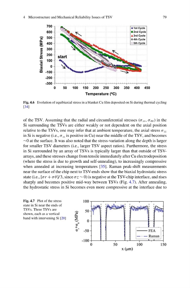
Fig. 4.6 Evolution of equibiaxial stress in a blanket Cu film deposited on Si during thermal cycling
[34]
of the TSV. Assuming that the radial and circumferential stresses (σ rr , σ θθ ) in the
Si surrounding the TSVs are either weakly or not dependent on the axial position
relative to the TSVs, one may infer that at ambient temperature, the axial stress σ zz
in Si is negative (i.e., σ zz is positive in Cu) near the middle of the TSV, and becomes
∼0 at the surface. It was also noted that the stress-variation along the depth is larger
for smaller TSV diameters (i.e., larger TSV aspect ratios). Furthermore, the stress
in Si surrounded by an array of TSVs is typically larger than that outside of TSVarrays, and these stresses change from tensile immediately after Cu electrodeposition
(where the stress is due to growth and self-annealing), to increasingly compressive
when annealed at increasing temperatures [35]. Raman peak-shift measurements
near the surface of the chip next to TSV-ends show that the biaxial hydrostatic stress
state (i.e., [σ r + σ θ]/ 3, since σ z ∼ 0) is negative at the TSV-chip interface, and rises
sharply and becomes positive mid-way between TSVs (Fig. 4.7). After annealing,
the hydrostatic stress in Si becomes even more compressive at the interface due to
Fig. 4.7 Plot of the stress
state in Si near the ends of
TSVs. Three TSVs are
shown, each as a vertical
band with intervening Si [20]
79
Fig. 4.6 Evolution of equibiaxial stress in a blanket Cu film deposited on Si during thermal cycling
[34]
of the TSV. Assuming that the radial and circumferential stresses (σ rr , σ θθ ) in the
Si surrounding the TSVs are either weakly or not dependent on the axial position
relative to the TSVs, one may infer that at ambient temperature, the axial stress σ zz
in Si is negative (i.e., σ zz is positive in Cu) near the middle of the TSV, and becomes
∼0 at the surface. It was also noted that the stress-variation along the depth is larger
for smaller TSV diameters (i.e., larger TSV aspect ratios). Furthermore, the stress
in Si surrounded by an array of TSVs is typically larger than that outside of TSVarrays, and these stresses change from tensile immediately after Cu electrodeposition
(where the stress is due to growth and self-annealing), to increasingly compressive
when annealed at increasing temperatures [35]. Raman peak-shift measurements
near the surface of the chip next to TSV-ends show that the biaxial hydrostatic stress
state (i.e., [σ r + σ θ]/ 3, since σ z ∼ 0) is negative at the TSV-chip interface, and rises
sharply and becomes positive mid-way between TSVs (Fig. 4.7). After annealing,
the hydrostatic stress in Si becomes even more compressive at the interface due to
Fig. 4.7 Plot of the stress
state in Si near the ends of
TSVs. Three TSVs are
shown, each as a vertical
band with intervening Si [20]