

78
P. Kumar et al.
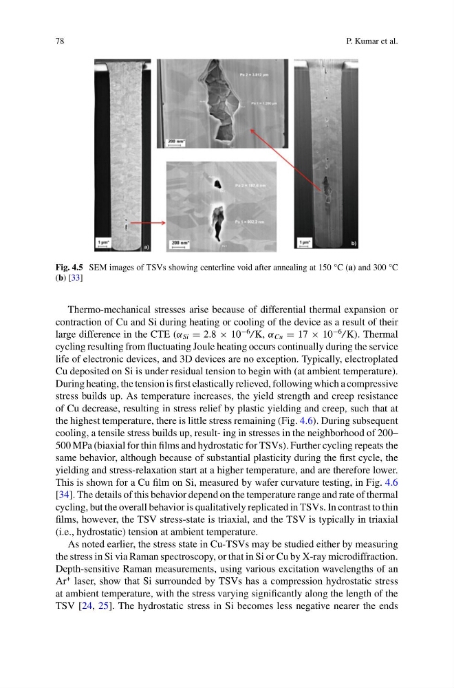
Fig. 4.5 SEM images of TSVs showing centerline void after annealing at 150 °C (a) and 300 °C
(b) [33]
Thermo-mechanical stresses arise because of differential thermal expansion or
contraction of Cu and Si during heating or cooling of the device as a result of their
large difference in the CTE (α Si = 2.8 × 10
−6 / K, α Cu = 17 × 10
−6 / K). Thermal
cycling resulting from fluctuating Joule heating occurs continually during the service
life of electronic devices, and 3D devices are no exception. Typically, electroplated
Cu deposited on Si is under residual tension to begin with (at ambient temperature).
During heating, the tension is first elastically relieved, following which a compressive
stress builds up. As temperature increases, the yield strength and creep resistance
of Cu decrease, resulting in stress relief by plastic yielding and creep, such that at
the highest temperature, there is little stress remaining (Fig. 4.6). During subsequent
cooling, a tensile stress builds up, result- ing in stresses in the neighborhood of 200–
500 MPa (biaxial for thin films and hydrostatic for TSVs). Further cycling repeats the
same behavior, although because of substantial plasticity during the first cycle, the
yielding and stress-relaxation start at a higher temperature, and are therefore lower.
This is shown for a Cu film on Si, measured by wafer curvature testing, in Fig. 4.6
[34]. The details of this behavior depend on the temperature range and rate of thermal
cycling, but the overall behavior is qualitatively replicated in TSVs. In contrast to thin
films, however, the TSV stress-state is triaxial, and the TSV is typically in triaxial
(i.e., hydrostatic) tension at ambient temperature.
As noted earlier, the stress state in Cu-TSVs may be studied either by measuring
the stress in Si via Raman spectroscopy, or that in Si or Cu by X-ray microdiffraction.
Depth-sensitive Raman measurements, using various excitation wavelengths of an
Ar
+ laser, show that Si surrounded by TSVs has a compression hydrostatic stress
at ambient temperature, with the stress varying significantly along the length of the
TSV [24, 25]. The hydrostatic stress in Si becomes less negative nearer the ends
P. Kumar et al.
Fig. 4.5 SEM images of TSVs showing centerline void after annealing at 150 °C (a) and 300 °C
(b) [33]
Thermo-mechanical stresses arise because of differential thermal expansion or
contraction of Cu and Si during heating or cooling of the device as a result of their
large difference in the CTE (α Si = 2.8 × 10
−6 / K, α Cu = 17 × 10
−6 / K). Thermal
cycling resulting from fluctuating Joule heating occurs continually during the service
life of electronic devices, and 3D devices are no exception. Typically, electroplated
Cu deposited on Si is under residual tension to begin with (at ambient temperature).
During heating, the tension is first elastically relieved, following which a compressive
stress builds up. As temperature increases, the yield strength and creep resistance
of Cu decrease, resulting in stress relief by plastic yielding and creep, such that at
the highest temperature, there is little stress remaining (Fig. 4.6). During subsequent
cooling, a tensile stress builds up, result- ing in stresses in the neighborhood of 200–
500 MPa (biaxial for thin films and hydrostatic for TSVs). Further cycling repeats the
same behavior, although because of substantial plasticity during the first cycle, the
yielding and stress-relaxation start at a higher temperature, and are therefore lower.
This is shown for a Cu film on Si, measured by wafer curvature testing, in Fig. 4.6
[34]. The details of this behavior depend on the temperature range and rate of thermal
cycling, but the overall behavior is qualitatively replicated in TSVs. In contrast to thin
films, however, the TSV stress-state is triaxial, and the TSV is typically in triaxial
(i.e., hydrostatic) tension at ambient temperature.
As noted earlier, the stress state in Cu-TSVs may be studied either by measuring
the stress in Si via Raman spectroscopy, or that in Si or Cu by X-ray microdiffraction.
Depth-sensitive Raman measurements, using various excitation wavelengths of an
Ar
+ laser, show that Si surrounded by TSVs has a compression hydrostatic stress
at ambient temperature, with the stress varying significantly along the length of the
TSV [24, 25]. The hydrostatic stress in Si becomes less negative nearer the ends