

66
P. Kumar et al.
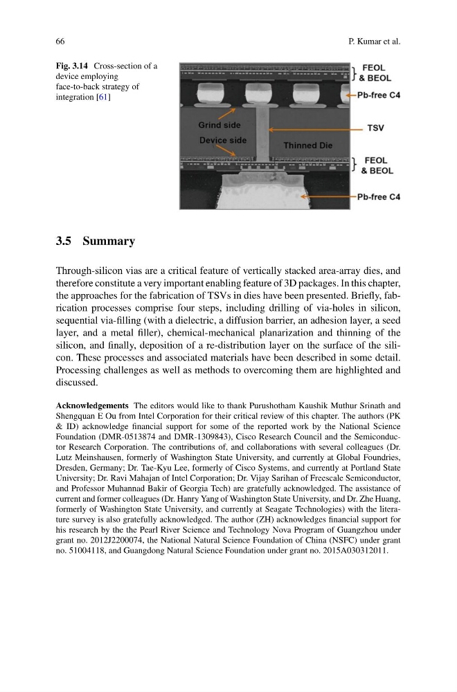
Fig. 3.14 Cross-section of a
device employing
face-to-back strategy of
integration [61]
3.5 Summary
Through-silicon vias are a critical feature of vertically stacked area-array dies, and
therefore constitute a very important enabling feature of 3D packages. In this chapter,
the approaches for the fabrication of TSVs in dies have been presented. Briefly, fabrication processes comprise four steps, including drilling of via-holes in silicon,
sequential via-filling (with a dielectric, a diffusion barrier, an adhesion layer, a seed
layer, and a metal filler), chemical-mechanical planarization and thinning of the
silicon, and finally, deposition of a re-distribution layer on the surface of the silicon. These processes and associated materials have been described in some detail.
Processing challenges as well as methods to overcoming them are highlighted and
discussed.
Acknowledgements The editors would like to thank Purushotham Kaushik Muthur Srinath and
Shengquan E Ou from Intel Corporation for their critical review of this chapter. The authors (PK
& ID) acknowledge financial support for some of the reported work by the National Science
Foundation (DMR-0513874 and DMR-1309843), Cisco Research Council and the Semiconductor Research Corporation. The contributions of, and collaborations with several colleagues (Dr.
Lutz Meinshausen, formerly of Washington State University, and currently at Global Foundries,
Dresden, Germany; Dr. Tae-Kyu Lee, formerly of Cisco Systems, and currently at Portland State
University; Dr. Ravi Mahajan of Intel Corporation; Dr. Vijay Sarihan of Freescale Semiconductor,
and Professor Muhannad Bakir of Georgia Tech) are gratefully acknowledged. The assistance of
current and former colleagues (Dr. Hanry Yang of Washington State University, and Dr. Zhe Huang,
formerly of Washington State University, and currently at Seagate Technologies) with the literature survey is also gratefully acknowledged. The author (ZH) acknowledges financial support for
his research by the the Pearl River Science and Technology Nova Program of Guangzhou under
grant no. 2012J2200074, the National Natural Science Foundation of China (NSFC) under grant
no. 51004118, and Guangdong Natural Science Foundation under grant no. 2015A030312011.
P. Kumar et al.
Fig. 3.14 Cross-section of a
device employing
face-to-back strategy of
integration [61]
3.5 Summary
Through-silicon vias are a critical feature of vertically stacked area-array dies, and
therefore constitute a very important enabling feature of 3D packages. In this chapter,
the approaches for the fabrication of TSVs in dies have been presented. Briefly, fabrication processes comprise four steps, including drilling of via-holes in silicon,
sequential via-filling (with a dielectric, a diffusion barrier, an adhesion layer, a seed
layer, and a metal filler), chemical-mechanical planarization and thinning of the
silicon, and finally, deposition of a re-distribution layer on the surface of the silicon. These processes and associated materials have been described in some detail.
Processing challenges as well as methods to overcoming them are highlighted and
discussed.
Acknowledgements The editors would like to thank Purushotham Kaushik Muthur Srinath and
Shengquan E Ou from Intel Corporation for their critical review of this chapter. The authors (PK
& ID) acknowledge financial support for some of the reported work by the National Science
Foundation (DMR-0513874 and DMR-1309843), Cisco Research Council and the Semiconductor Research Corporation. The contributions of, and collaborations with several colleagues (Dr.
Lutz Meinshausen, formerly of Washington State University, and currently at Global Foundries,
Dresden, Germany; Dr. Tae-Kyu Lee, formerly of Cisco Systems, and currently at Portland State
University; Dr. Ravi Mahajan of Intel Corporation; Dr. Vijay Sarihan of Freescale Semiconductor,
and Professor Muhannad Bakir of Georgia Tech) are gratefully acknowledged. The assistance of
current and former colleagues (Dr. Hanry Yang of Washington State University, and Dr. Zhe Huang,
formerly of Washington State University, and currently at Seagate Technologies) with the literature survey is also gratefully acknowledged. The author (ZH) acknowledges financial support for
his research by the the Pearl River Science and Technology Nova Program of Guangzhou under
grant no. 2012J2200074, the National Natural Science Foundation of China (NSFC) under grant
no. 51004118, and Guangdong Natural Science Foundation under grant no. 2015A030312011.