

3 Materials and Processing of TSV
59
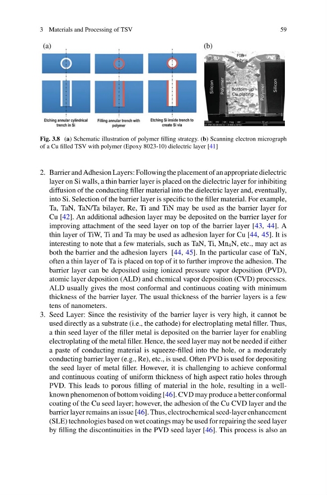
Fig. 3.8 (a) Schematic illustration of polymer filling strategy. (b) Scanning electron micrograph
of a Cu filled TSV with polymer (Epoxy 8023-10) dielectric layer [41]
2. Barrier and Adhesion Layers: Following the placement of an appropriate dielectric
layer on Si walls, a thin barrier layer is placed on the dielectric layer for inhibiting
diffusion of the conducting filler material into the dielectric layer and, eventually,
into Si. Selection of the barrier layer is specific to the filler material. For example,
Ta, TaN, TaN/Ta bilayer, Re, Ti and TiN may be used as the barrier layer for
Cu [42]. An additional adhesion layer may be deposited on the barrier layer for
improving attachment of the seed layer on top of the barrier layer [43, 44]. A
thin layer of TiW, Ti and Ta may be used as adhesion layer for Cu [44, 45]. It is
interesting to note that a few materials, such as TaN, Ti, Mn 4 N, etc., may act as
both the barrier and the adhesion layers [44, 45]. In the particular case of TaN,
often a thin layer of Ta is placed on top of it to further improve the adhesion. The
barrier layer can be deposited using ionized pressure vapor deposition (PVD),
atomic layer deposition (ALD) and chemical vapor deposition (CVD) processes.
ALD usually gives the most conformal and continuous coating with minimum
thickness of the barrier layer. The usual thickness of the barrier layers is a few
tens of nanometers.
3. Seed Layer: Since the resistivity of the barrier layer is very high, it cannot be
used directly as a substrate (i.e., the cathode) for electroplating metal filler. Thus,
a thin seed layer of the filler metal is deposited on the barrier layer for enabling
electroplating of the metal filler. Hence, the seed layer may not be needed if either
a paste of conducting material is squeeze-filled into the hole, or a moderately
conducting barrier layer (e.g., Re), etc., is used. Often PVD is used for depositing
the seed layer of metal filler. However, it is challenging to achieve conformal
and continuous coating of uniform thickness of high aspect ratio holes through
PVD. This leads to porous filling of material in the hole, resulting in a wellknown phenomenon of bottom voiding [46]. CVD may produce a better conformal
coating of the Cu seed layer; however, the adhesion of the Cu CVD layer and the
barrier layer remains an issue [46]. Thus, electrochemical seed-layer enhancement
(SLE) technologies based on wet coatings may be used for repairing the seed layer
by filling the discontinuities in the PVD seed layer [46]. This process is also an
59
Fig. 3.8 (a) Schematic illustration of polymer filling strategy. (b) Scanning electron micrograph
of a Cu filled TSV with polymer (Epoxy 8023-10) dielectric layer [41]
2. Barrier and Adhesion Layers: Following the placement of an appropriate dielectric
layer on Si walls, a thin barrier layer is placed on the dielectric layer for inhibiting
diffusion of the conducting filler material into the dielectric layer and, eventually,
into Si. Selection of the barrier layer is specific to the filler material. For example,
Ta, TaN, TaN/Ta bilayer, Re, Ti and TiN may be used as the barrier layer for
Cu [42]. An additional adhesion layer may be deposited on the barrier layer for
improving attachment of the seed layer on top of the barrier layer [43, 44]. A
thin layer of TiW, Ti and Ta may be used as adhesion layer for Cu [44, 45]. It is
interesting to note that a few materials, such as TaN, Ti, Mn 4 N, etc., may act as
both the barrier and the adhesion layers [44, 45]. In the particular case of TaN,
often a thin layer of Ta is placed on top of it to further improve the adhesion. The
barrier layer can be deposited using ionized pressure vapor deposition (PVD),
atomic layer deposition (ALD) and chemical vapor deposition (CVD) processes.
ALD usually gives the most conformal and continuous coating with minimum
thickness of the barrier layer. The usual thickness of the barrier layers is a few
tens of nanometers.
3. Seed Layer: Since the resistivity of the barrier layer is very high, it cannot be
used directly as a substrate (i.e., the cathode) for electroplating metal filler. Thus,
a thin seed layer of the filler metal is deposited on the barrier layer for enabling
electroplating of the metal filler. Hence, the seed layer may not be needed if either
a paste of conducting material is squeeze-filled into the hole, or a moderately
conducting barrier layer (e.g., Re), etc., is used. Often PVD is used for depositing
the seed layer of metal filler. However, it is challenging to achieve conformal
and continuous coating of uniform thickness of high aspect ratio holes through
PVD. This leads to porous filling of material in the hole, resulting in a wellknown phenomenon of bottom voiding [46]. CVD may produce a better conformal
coating of the Cu seed layer; however, the adhesion of the Cu CVD layer and the
barrier layer remains an issue [46]. Thus, electrochemical seed-layer enhancement
(SLE) technologies based on wet coatings may be used for repairing the seed layer
by filling the discontinuities in the PVD seed layer [46]. This process is also an