

3 Materials and Processing of TSV
53
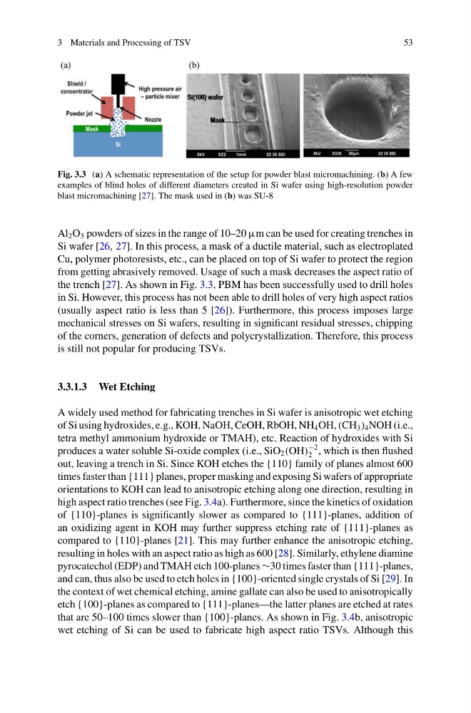
Fig. 3.3 (a) A schematic representation of the setup for powder blast micromachining. (b) A few
examples of blind holes of different diameters created in Si wafer using high-resolution powder
blast micromachining [27]. The mask used in (b) was SU-8
Al 2 O 3 powders of sizes in the range of 10–20 µm can be used for creating trenches in
Si wafer [26, 27]. In this process, a mask of a ductile material, such as electroplated
Cu, polymer photoresists, etc., can be placed on top of Si wafer to protect the region
from getting abrasively removed. Usage of such a mask decreases the aspect ratio of
the trench [27]. As shown in Fig. 3.3, PBM has been successfully used to drill holes
in Si. However, this process has not been able to drill holes of very high aspect ratios
(usually aspect ratio is less than 5 [26]). Furthermore, this process imposes large
mechanical stresses on Si wafers, resulting in significant residual stresses, chipping
of the corners, generation of defects and polycrystallization. Therefore, this process
is still not popular for producing TSVs.
3.3.1.3 Wet Etching
A widely used method for fabricating trenches in Si wafer is anisotropic wet etching
of Si using hydroxides, e.g., KOH, NaOH, CeOH, RbOH, NH 4 OH, (CH 3 ) 4 NOH (i.e.,
tetra methyl ammonium hydroxide or TMAH), etc. Reaction of hydroxides with Si
produces a water soluble Si-oxide complex (i.e., SiO 2 (OH)
−2
2 , which is then flushed
out, leaving a trench in Si. Since KOH etches the {110} family of planes almost 600
times faster than {111} planes, proper masking and exposing Si wafers of appropriate
orientations to KOH can lead to anisotropic etching along one direction, resulting in
high aspect ratio trenches (see Fig. 3.4a). Furthermore, since the kinetics of oxidation
of {110}-planes is significantly slower as compared to {111}-planes, addition of
an oxidizing agent in KOH may further suppress etching rate of {111}-planes as
compared to {110}-planes [21]. This may further enhance the anisotropic etching,
resulting in holes with an aspect ratio as high as 600 [28]. Similarly, ethylene diamine
pyrocatechol (EDP) and TMAH etch 100-planes ∼30 times faster than {111}-planes,
and can, thus also be used to etch holes in {100}-oriented single crystals of Si [29]. In
the context of wet chemical etching, amine gallate can also be used to anisotropically
etch {100}-planes as compared to {111}-planes—the latter planes are etched at rates
that are 50–100 times slower than {100}-planes. As shown in Fig. 3.4b, anisotropic
wet etching of Si can be used to fabricate high aspect ratio TSVs. Although this
53
Fig. 3.3 (a) A schematic representation of the setup for powder blast micromachining. (b) A few
examples of blind holes of different diameters created in Si wafer using high-resolution powder
blast micromachining [27]. The mask used in (b) was SU-8
Al 2 O 3 powders of sizes in the range of 10–20 µm can be used for creating trenches in
Si wafer [26, 27]. In this process, a mask of a ductile material, such as electroplated
Cu, polymer photoresists, etc., can be placed on top of Si wafer to protect the region
from getting abrasively removed. Usage of such a mask decreases the aspect ratio of
the trench [27]. As shown in Fig. 3.3, PBM has been successfully used to drill holes
in Si. However, this process has not been able to drill holes of very high aspect ratios
(usually aspect ratio is less than 5 [26]). Furthermore, this process imposes large
mechanical stresses on Si wafers, resulting in significant residual stresses, chipping
of the corners, generation of defects and polycrystallization. Therefore, this process
is still not popular for producing TSVs.
3.3.1.3 Wet Etching
A widely used method for fabricating trenches in Si wafer is anisotropic wet etching
of Si using hydroxides, e.g., KOH, NaOH, CeOH, RbOH, NH 4 OH, (CH 3 ) 4 NOH (i.e.,
tetra methyl ammonium hydroxide or TMAH), etc. Reaction of hydroxides with Si
produces a water soluble Si-oxide complex (i.e., SiO 2 (OH)
−2
2 , which is then flushed
out, leaving a trench in Si. Since KOH etches the {110} family of planes almost 600
times faster than {111} planes, proper masking and exposing Si wafers of appropriate
orientations to KOH can lead to anisotropic etching along one direction, resulting in
high aspect ratio trenches (see Fig. 3.4a). Furthermore, since the kinetics of oxidation
of {110}-planes is significantly slower as compared to {111}-planes, addition of
an oxidizing agent in KOH may further suppress etching rate of {111}-planes as
compared to {110}-planes [21]. This may further enhance the anisotropic etching,
resulting in holes with an aspect ratio as high as 600 [28]. Similarly, ethylene diamine
pyrocatechol (EDP) and TMAH etch 100-planes ∼30 times faster than {111}-planes,
and can, thus also be used to etch holes in {100}-oriented single crystals of Si [29]. In
the context of wet chemical etching, amine gallate can also be used to anisotropically
etch {100}-planes as compared to {111}-planes—the latter planes are etched at rates
that are 50–100 times slower than {100}-planes. As shown in Fig. 3.4b, anisotropic
wet etching of Si can be used to fabricate high aspect ratio TSVs. Although this