

52
P. Kumar et al.
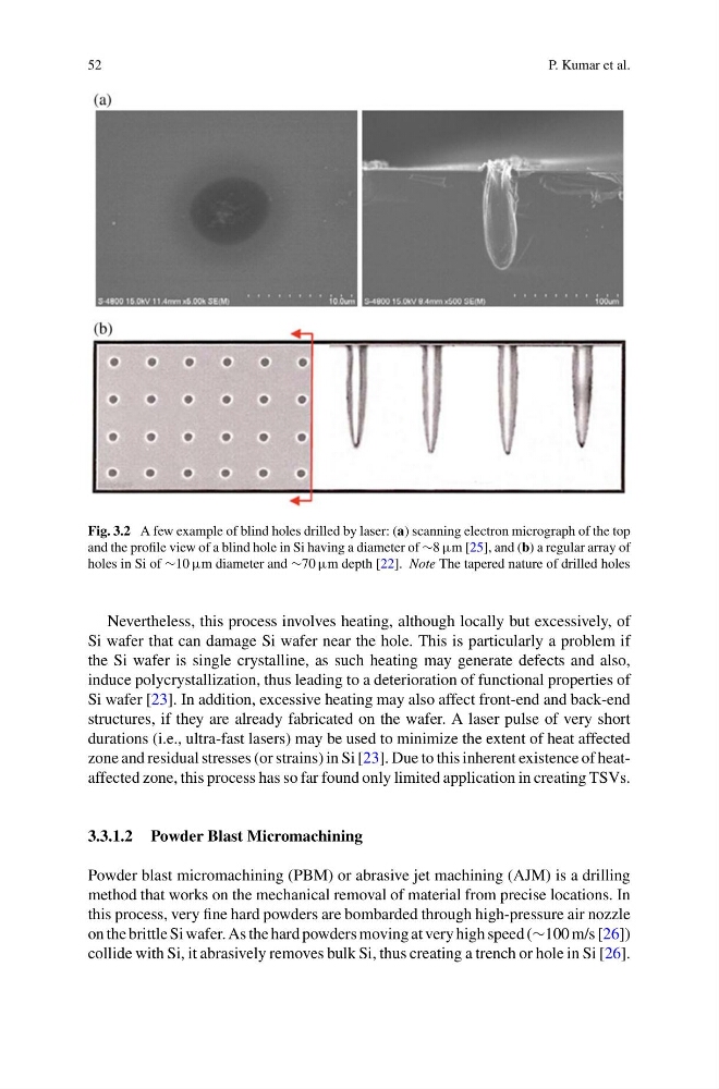
Fig. 3.2 A few example of blind holes drilled by laser: (a) scanning electron micrograph of the top
and the profile view of a blind hole in Si having a diameter of ∼8 µm [25], and (b) a regular array of
holes in Si of ∼10 µm diameter and ∼70 µm depth [22]. Note The tapered nature of drilled holes
Nevertheless, this process involves heating, although locally but excessively, of
Si wafer that can damage Si wafer near the hole. This is particularly a problem if
the Si wafer is single crystalline, as such heating may generate defects and also,
induce polycrystallization, thus leading to a deterioration of functional properties of
Si wafer [23]. In addition, excessive heating may also affect front-end and back-end
structures, if they are already fabricated on the wafer. A laser pulse of very short
durations (i.e., ultra-fast lasers) may be used to minimize the extent of heat affected
zone and residual stresses (or strains) in Si [23]. Due to this inherent existence of heataffected zone, this process has so far found only limited application in creating TSVs.
3.3.1.2 Powder Blast Micromachining
Powder blast micromachining (PBM) or abrasive jet machining (AJM) is a drilling
method that works on the mechanical removal of material from precise locations. In
this process, very fine hard powders are bombarded through high-pressure air nozzle
on the brittle Si wafer. As the hard powders moving at very high speed (∼100 m/s [26])
collide with Si, it abrasively removes bulk Si, thus creating a trench or hole in Si [26].
P. Kumar et al.
Fig. 3.2 A few example of blind holes drilled by laser: (a) scanning electron micrograph of the top
and the profile view of a blind hole in Si having a diameter of ∼8 µm [25], and (b) a regular array of
holes in Si of ∼10 µm diameter and ∼70 µm depth [22]. Note The tapered nature of drilled holes
Nevertheless, this process involves heating, although locally but excessively, of
Si wafer that can damage Si wafer near the hole. This is particularly a problem if
the Si wafer is single crystalline, as such heating may generate defects and also,
induce polycrystallization, thus leading to a deterioration of functional properties of
Si wafer [23]. In addition, excessive heating may also affect front-end and back-end
structures, if they are already fabricated on the wafer. A laser pulse of very short
durations (i.e., ultra-fast lasers) may be used to minimize the extent of heat affected
zone and residual stresses (or strains) in Si [23]. Due to this inherent existence of heataffected zone, this process has so far found only limited application in creating TSVs.
3.3.1.2 Powder Blast Micromachining
Powder blast micromachining (PBM) or abrasive jet machining (AJM) is a drilling
method that works on the mechanical removal of material from precise locations. In
this process, very fine hard powders are bombarded through high-pressure air nozzle
on the brittle Si wafer. As the hard powders moving at very high speed (∼100 m/s [26])
collide with Si, it abrasively removes bulk Si, thus creating a trench or hole in Si [26].