

18 Fault Isolation and Failure Analysis of 3D Packaging
599
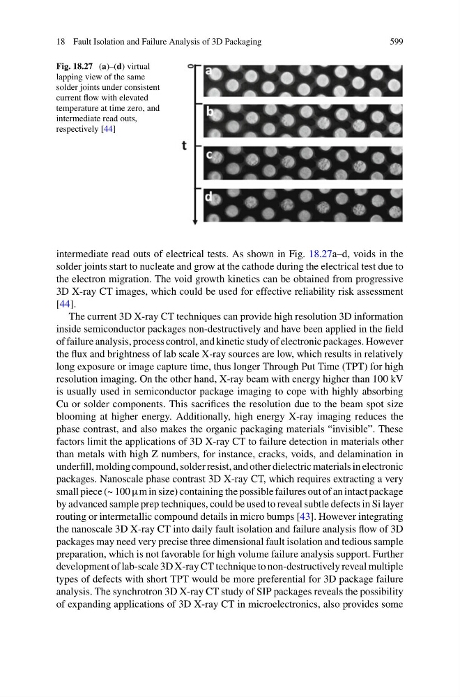
Fig. 18.27 (a)–(d) virtual
lapping view of the same
solder joints under consistent
current flow with elevated
temperature at time zero, and
intermediate read outs,
respectively [44]
intermediate read outs of electrical tests. As shown in Fig. 18.27a–d, voids in the
solder joints start to nucleate and grow at the cathode during the electrical test due to
the electron migration. The void growth kinetics can be obtained from progressive
3D X-ray CT images, which could be used for effective reliability risk assessment
[44].
The current 3D X-ray CT techniques can provide high resolution 3D information
inside semiconductor packages non-destructively and have been applied in the field
of failure analysis, process control, and kinetic study of electronic packages. However
the flux and brightness of lab scale X-ray sources are low, which results in relatively
long exposure or image capture time, thus longer Through Put Time (TPT) for high
resolution imaging. On the other hand, X-ray beam with energy higher than 100 kV
is usually used in semiconductor package imaging to cope with highly absorbing
Cu or solder components. This sacrifices the resolution due to the beam spot size
blooming at higher energy. Additionally, high energy X-ray imaging reduces the
phase contrast, and also makes the organic packaging materials “invisible”. These
factors limit the applications of 3D X-ray CT to failure detection in materials other
than metals with high Z numbers, for instance, cracks, voids, and delamination in
underfill, molding compound, solder resist, and other dielectric materials in electronic
packages. Nanoscale phase contrast 3D X-ray CT, which requires extracting a very
small piece (~ 100 μm in size) containing the possible failures out of an intact package
by advanced sample prep techniques, could be used to reveal subtle defects in Si layer
routing or intermetallic compound details in micro bumps [43]. However integrating
the nanoscale 3D X-ray CT into daily fault isolation and failure analysis flow of 3D
packages may need very precise three dimensional fault isolation and tedious sample
preparation, which is not favorable for high volume failure analysis support. Further
development of lab-scale 3D X-ray CT technique to non-destructively reveal multiple
types of defects with short TPT would be more preferential for 3D package failure
analysis. The synchrotron 3D X-ray CT study of SIP packages reveals the possibility
of expanding applications of 3D X-ray CT in microelectronics, also provides some