

600
Y. Li and D. Goyal
suggestions to the development of next generation lab-scale 3D X-ray CT systems
[44, 47].
18.4 The Application of Sample Preparation and Material
Analysis Techniques to 3D microelectronic packages
18.4.1 Sample Preparation Techniques
Root cause understanding of failures is critical for process improvement and optimization during product development, which typically needs destructive failure analysis, such as cross sectional data, to disclose the details of defects. As interconnects in
3D package could be as small as a few micrometers in diameter, it is very challenging
to get good alignment as well as artifact free finish using conventional mechanical
cross sectional techniques. On the other hand, it is very time consuming to cross
section TSVs with more than one hundred micrometers in length by the conventional focused ion beam (FIB) technique [48]. A couple of advanced cross section
techniques, for example plasma-FIB, femtosecond (fs) and nanosecond (ns) laser
ablation, and broad-beam ion milling, are developed in the industry to fill in the
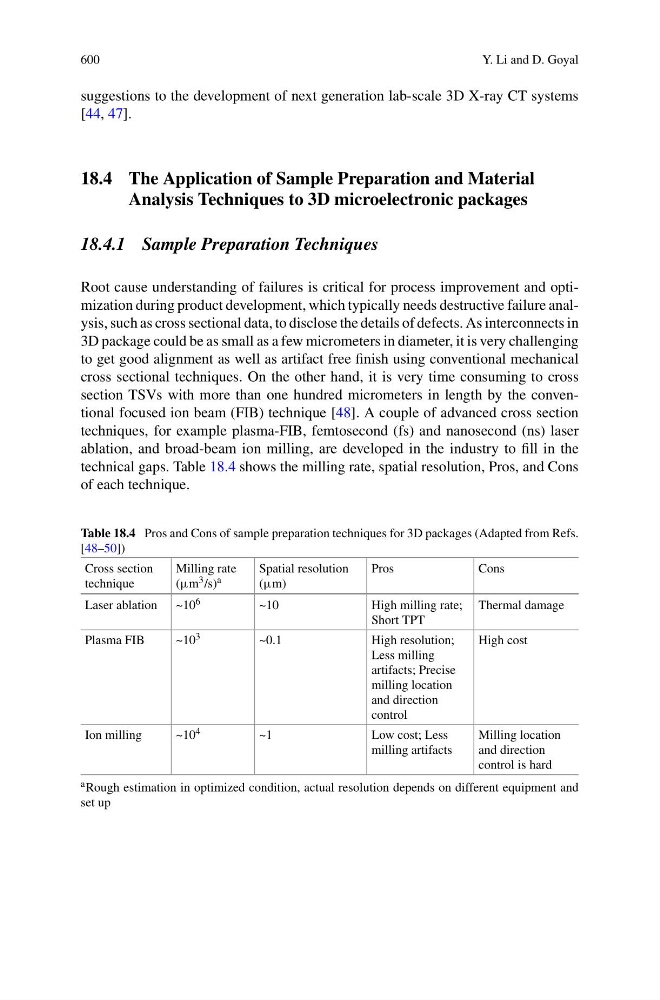
technical gaps. Table 18.4 shows the milling rate, spatial resolution, Pros, and Cons
of each technique.
Table 18.4 Pros and Cons of sample preparation techniques for 3D packages (Adapted from Refs.
[48–50])
Cross section
technique
Milling rate
(μm 3 /s) a
Spatial resolution
(μm)
Pros
Cons
Laser ablation ~10 6
~10
High milling rate;
Short TPT
Thermal damage
Plasma FIB
~10 3
~0.1
High resolution;
Less milling
artifacts; Precise
milling location
and direction
control
High cost
Ion milling
~10 4
~1
Low cost; Less
milling artifacts
Milling location
and direction
control is hard
a Rough estimation in optimized condition, actual resolution depends on different equipment and
set up