

598
Y. Li and D. Goyal
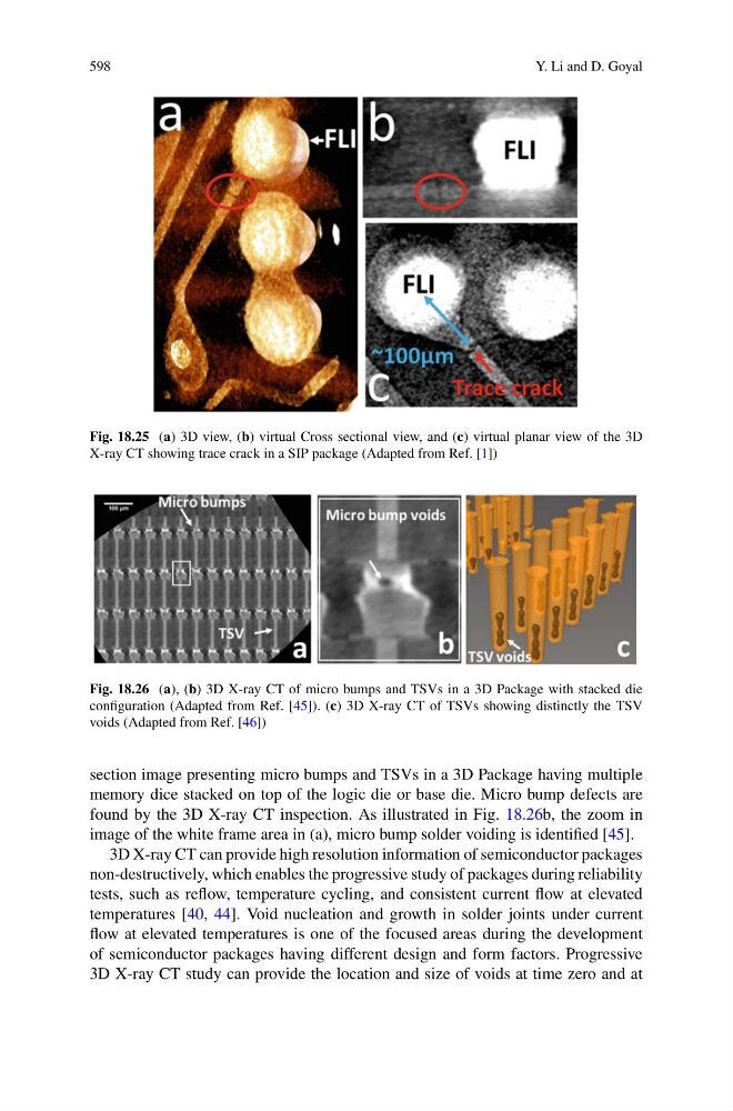
Fig. 18.25 (a) 3D view, (b) virtual Cross sectional view, and (c) virtual planar view of the 3D
X-ray CT showing trace crack in a SIP package (Adapted from Ref. [1])
Fig. 18.26 (a), (b) 3D X-ray CT of micro bumps and TSVs in a 3D Package with stacked die
configuration (Adapted from Ref. [45]). (c) 3D X-ray CT of TSVs showing distinctly the TSV
voids (Adapted from Ref. [46])
section image presenting micro bumps and TSVs in a 3D Package having multiple
memory dice stacked on top of the logic die or base die. Micro bump defects are
found by the 3D X-ray CT inspection. As illustrated in Fig. 18.26b, the zoom in
image of the white frame area in (a), micro bump solder voiding is identified [45].
3D X-ray CT can provide high resolution information of semiconductor packages
non-destructively, which enables the progressive study of packages during reliability
tests, such as reflow, temperature cycling, and consistent current flow at elevated
temperatures [40, 44]. Void nucleation and growth in solder joints under current
flow at elevated temperatures is one of the focused areas during the development
of semiconductor packages having different design and form factors. Progressive
3D X-ray CT study can provide the location and size of voids at time zero and at