

596
Y. Li and D. Goyal
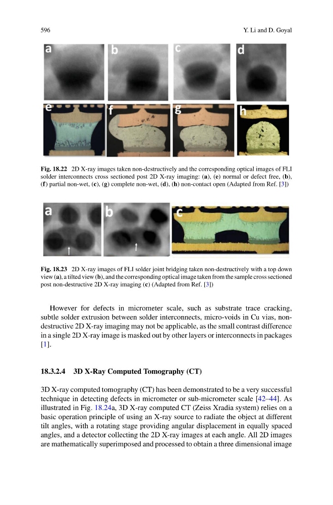
Fig. 18.22 2D X-ray images taken non-destructively and the corresponding optical images of FLI
solder interconnects cross sectioned post 2D X-ray imaging: (a), (e) normal or defect free, (b),
(f) partial non-wet, (c), (g) complete non-wet, (d), (h) non-contact open (Adapted from Ref. [3])
Fig. 18.23 2D X-ray images of FLI solder joint bridging taken non-destructively with a top down
view (a), a tilted view (b), and the corresponding optical image taken from the sample cross sectioned
post non-destructive 2D X-ray imaging (c) (Adapted from Ref. [3])
However for defects in micrometer scale, such as substrate trace cracking,
subtle solder extrusion between solder interconnects, micro-voids in Cu vias, nondestructive 2D X-ray imaging may not be applicable, as the small contrast difference
in a single 2D X-ray image is masked out by other layers or interconnects in packages
[1].
18.3.2.4 3D X-Ray Computed Tomography (CT)
3D X-ray computed tomography (CT) has been demonstrated to be a very successful
technique in detecting defects in micrometer or sub-micrometer scale [42–44]. As
illustrated in Fig. 18.24a, 3D X-ray computed CT (Zeiss Xradia system) relies on a
basic operation principle of using an X-ray source to radiate the object at different
tilt angles, with a rotating stage providing angular displacement in equally spaced
angles, and a detector collecting the 2D X-ray images at each angle. All 2D images
are mathematically superimposed and processed to obtain a three dimensional image