

576
Y. Li and D. Goyal
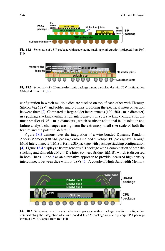
Fig. 18.1 Schematic of a SIP package with a packaging stacking configuration (Adapted from Ref.
[1])
Fig. 18.2 Schematic of a 3D microelectronic package having a stacked die with TSV configuration
(Adapted from Ref. [3])
configuration in which multiple dice are stacked on top of each other with Through
Silicon Via (TSV) and solder micro bumps providing the electrical interconnection
between them [2]. Compared to large solder interconnects (100–500 μm in diameter)
in a package stacking configuration, interconnects in a die stacking configuration are
much smaller (5–25 μm in diameters), which results in additional fault isolation and
failure analysis challenges arising from the extremely small size scale of both the
feature and the potential defect [3].
Figure 18.3 demonstrates the integration of a wire bonded Dynamic Random
Access Memory (DRAM) package onto a molded flip chip CPU package by Through
Mold Interconnects (TMI) to form a 3D package with package stacking configuration
[4]. Figure 18.4 displays a heterogeneous 3D package with a combination of both die
stacking and Embedded Multi-Die Inter-connect Bridge (EMIB), which is discussed
in both Chaps. 1 and 2 as an alternative approach to provide localized high density
interconnects between dice without TSVs [5]. A couple of High Bandwidth Memory
Fig. 18.3 Schematic of a 3D microelectronic package with a package stacking configuration
demonstrating the integration of a wire bonded DRAM package onto a flip chip CPU package
through TMI (Adapted from Ref. [4])
Y. Li and D. Goyal
Fig. 18.1 Schematic of a SIP package with a packaging stacking configuration (Adapted from Ref.
[1])
Fig. 18.2 Schematic of a 3D microelectronic package having a stacked die with TSV configuration
(Adapted from Ref. [3])
configuration in which multiple dice are stacked on top of each other with Through
Silicon Via (TSV) and solder micro bumps providing the electrical interconnection
between them [2]. Compared to large solder interconnects (100–500 μm in diameter)
in a package stacking configuration, interconnects in a die stacking configuration are
much smaller (5–25 μm in diameters), which results in additional fault isolation and
failure analysis challenges arising from the extremely small size scale of both the
feature and the potential defect [3].
Figure 18.3 demonstrates the integration of a wire bonded Dynamic Random
Access Memory (DRAM) package onto a molded flip chip CPU package by Through
Mold Interconnects (TMI) to form a 3D package with package stacking configuration
[4]. Figure 18.4 displays a heterogeneous 3D package with a combination of both die
stacking and Embedded Multi-Die Inter-connect Bridge (EMIB), which is discussed
in both Chaps. 1 and 2 as an alternative approach to provide localized high density
interconnects between dice without TSVs [5]. A couple of High Bandwidth Memory
Fig. 18.3 Schematic of a 3D microelectronic package with a package stacking configuration
demonstrating the integration of a wire bonded DRAM package onto a flip chip CPU package
through TMI (Adapted from Ref. [4])