

18 Fault Isolation and Failure Analysis of 3D Packaging
577
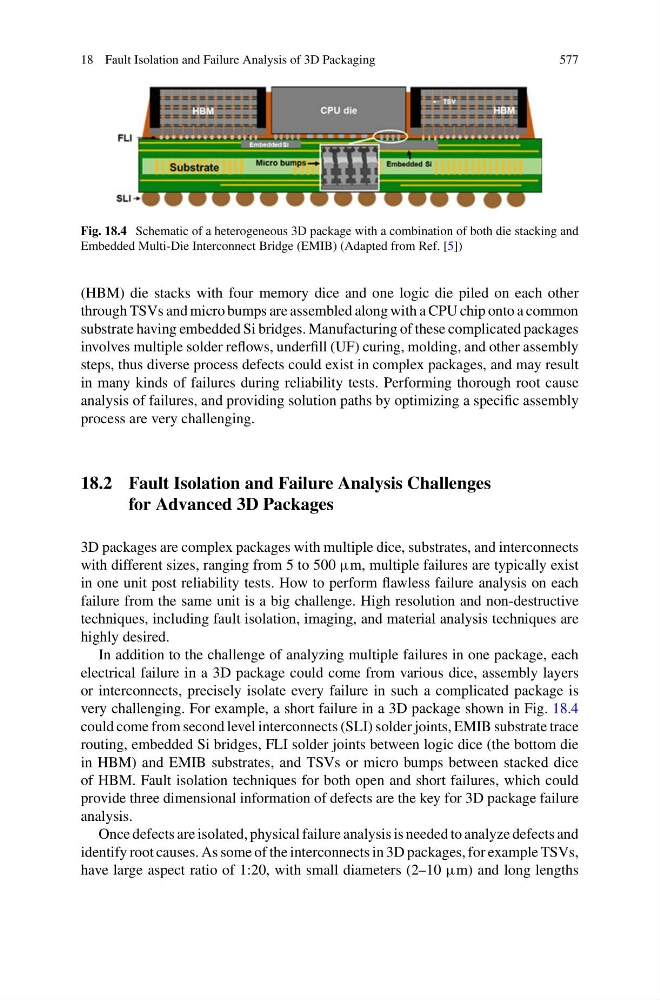
Fig. 18.4 Schematic of a heterogeneous 3D package with a combination of both die stacking and
Embedded Multi-Die Interconnect Bridge (EMIB) (Adapted from Ref. [5])
(HBM) die stacks with four memory dice and one logic die piled on each other
through TSVs and micro bumps are assembled along with a CPU chip onto a common
substrate having embedded Si bridges. Manufacturing of these complicated packages
involves multiple solder reflows, underfill (UF) curing, molding, and other assembly
steps, thus diverse process defects could exist in complex packages, and may result
in many kinds of failures during reliability tests. Performing thorough root cause
analysis of failures, and providing solution paths by optimizing a specific assembly
process are very challenging.
18.2 Fault Isolation and Failure Analysis Challenges
for Advanced 3D Packages
3D packages are complex packages with multiple dice, substrates, and interconnects
with different sizes, ranging from 5 to 500 μm, multiple failures are typically exist
in one unit post reliability tests. How to perform flawless failure analysis on each
failure from the same unit is a big challenge. High resolution and non-destructive
techniques, including fault isolation, imaging, and material analysis techniques are
highly desired.
In addition to the challenge of analyzing multiple failures in one package, each
electrical failure in a 3D package could come from various dice, assembly layers
or interconnects, precisely isolate every failure in such a complicated package is
very challenging. For example, a short failure in a 3D package shown in Fig. 18.4
could come from second level interconnects (SLI) solder joints, EMIB substrate trace
routing, embedded Si bridges, FLI solder joints between logic dice (the bottom die
in HBM) and EMIB substrates, and TSVs or micro bumps between stacked dice
of HBM. Fault isolation techniques for both open and short failures, which could
provide three dimensional information of defects are the key for 3D package failure
analysis.
Once defects are isolated, physical failure analysis is needed to analyze defects and
identify root causes. As some of the interconnects in 3D packages, for example TSVs,
have large aspect ratio of 1:20, with small diameters (2–10 μm) and long lengths
577
Fig. 18.4 Schematic of a heterogeneous 3D package with a combination of both die stacking and
Embedded Multi-Die Interconnect Bridge (EMIB) (Adapted from Ref. [5])
(HBM) die stacks with four memory dice and one logic die piled on each other
through TSVs and micro bumps are assembled along with a CPU chip onto a common
substrate having embedded Si bridges. Manufacturing of these complicated packages
involves multiple solder reflows, underfill (UF) curing, molding, and other assembly
steps, thus diverse process defects could exist in complex packages, and may result
in many kinds of failures during reliability tests. Performing thorough root cause
analysis of failures, and providing solution paths by optimizing a specific assembly
process are very challenging.
18.2 Fault Isolation and Failure Analysis Challenges
for Advanced 3D Packages
3D packages are complex packages with multiple dice, substrates, and interconnects
with different sizes, ranging from 5 to 500 μm, multiple failures are typically exist
in one unit post reliability tests. How to perform flawless failure analysis on each
failure from the same unit is a big challenge. High resolution and non-destructive
techniques, including fault isolation, imaging, and material analysis techniques are
highly desired.
In addition to the challenge of analyzing multiple failures in one package, each
electrical failure in a 3D package could come from various dice, assembly layers
or interconnects, precisely isolate every failure in such a complicated package is
very challenging. For example, a short failure in a 3D package shown in Fig. 18.4
could come from second level interconnects (SLI) solder joints, EMIB substrate trace
routing, embedded Si bridges, FLI solder joints between logic dice (the bottom die
in HBM) and EMIB substrates, and TSVs or micro bumps between stacked dice
of HBM. Fault isolation techniques for both open and short failures, which could
provide three dimensional information of defects are the key for 3D package failure
analysis.
Once defects are isolated, physical failure analysis is needed to analyze defects and
identify root causes. As some of the interconnects in 3D packages, for example TSVs,
have large aspect ratio of 1:20, with small diameters (2–10 μm) and long lengths