

17 Interconnect Quality and Reliability of 3D Packaging
567
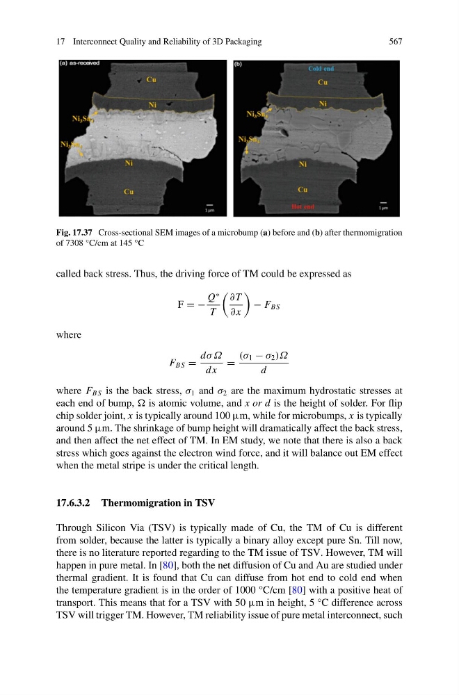
Fig. 17.37 Cross-sectional SEM images of a microbump (a) before and (b) after thermomigration
of 7308 °C/cm at 145 °C
called back stress. Thus, the driving force of TM could be expressed as
F = −
Q
∗
T
∂ T
∂ x
− F BS
where
F BS =
dσ Ω
dx
=
(σ 1 − σ 2 )Ω
d
where F BS is the back stress, σ 1 and σ 2 are the maximum hydrostatic stresses at
each end of bump, is atomic volume, and x or d is the height of solder. For flip
chip solder joint, x is typically around 100 μm, while for microbumps, x is typically
around 5 μm. The shrinkage of bump height will dramatically affect the back stress,
and then affect the net effect of TM. In EM study, we note that there is also a back
stress which goes against the electron wind force, and it will balance out EM effect
when the metal stripe is under the critical length.
17.6.3.2 Thermomigration in TSV
Through Silicon Via (TSV) is typically made of Cu, the TM of Cu is different
from solder, because the latter is typically a binary alloy except pure Sn. Till now,
there is no literature reported regarding to the TM issue of TSV. However, TM will
happen in pure metal. In [80], both the net diffusion of Cu and Au are studied under
thermal gradient. It is found that Cu can diffuse from hot end to cold end when
the temperature gradient is in the order of 1000 °C/cm [80] with a positive heat of
transport. This means that for a TSV with 50 μm in height, 5 °C difference across
TSV will trigger TM. However, TM reliability issue of pure metal interconnect, such
567
Fig. 17.37 Cross-sectional SEM images of a microbump (a) before and (b) after thermomigration
of 7308 °C/cm at 145 °C
called back stress. Thus, the driving force of TM could be expressed as
F = −
Q
∗
T
∂ T
∂ x
− F BS
where
F BS =
dσ Ω
dx
=
(σ 1 − σ 2 )Ω
d
where F BS is the back stress, σ 1 and σ 2 are the maximum hydrostatic stresses at
each end of bump, is atomic volume, and x or d is the height of solder. For flip
chip solder joint, x is typically around 100 μm, while for microbumps, x is typically
around 5 μm. The shrinkage of bump height will dramatically affect the back stress,
and then affect the net effect of TM. In EM study, we note that there is also a back
stress which goes against the electron wind force, and it will balance out EM effect
when the metal stripe is under the critical length.
17.6.3.2 Thermomigration in TSV
Through Silicon Via (TSV) is typically made of Cu, the TM of Cu is different
from solder, because the latter is typically a binary alloy except pure Sn. Till now,
there is no literature reported regarding to the TM issue of TSV. However, TM will
happen in pure metal. In [80], both the net diffusion of Cu and Au are studied under
thermal gradient. It is found that Cu can diffuse from hot end to cold end when
the temperature gradient is in the order of 1000 °C/cm [80] with a positive heat of
transport. This means that for a TSV with 50 μm in height, 5 °C difference across
TSV will trigger TM. However, TM reliability issue of pure metal interconnect, such