

568
Y. Wang et al.
as Cu interconnects, is not well reported. The reason is possibly related to back stress.
Because device is usually working at 100 °C, this temperature is too low for creep
to take place in Cu. When TM drives more Cu atoms from the hot side into the cold
side (or the reverse direction depending on the heat of transport), the stress will build
up at the end where atomic accumulation occurs, and then the stress gradient will
produce an atomic flux of Cu against the TM.
Since TSV is connected to the redistribution layer at both ends, and the current
crowding will occur at the interfaces, it is possible that the local Joule heating due
to current crowding will create a temperature gradient that is high enough for TM to
occur. Meanwhile, due to the high power density, and poor heat dissipation in 3D IC,
the working temperature around TSV might be high enough for creep to take place
in Cu, in which case the back stress may not play a role.
17.6.3.3 Thermomigration Induced by Thermal Cross-Talk
In 2.5D IC packaging design, a layer of Si interposer is used in between dies and
substrate to mitigate the chip-packaging interaction. Nevertheless, this new design
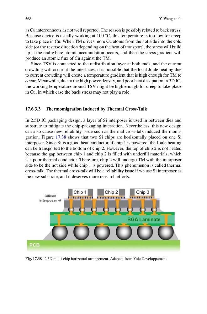
can also cause new reliability issue such as thermal cross-talk induced thermomigration. Figure 17.38 shows that two Si chips are horizontally placed on one Si
interposer. Since Si is a good heat conductor, if chip 1 is powered, the Joule heating
can be transported to the bottom of chip 2. However, the top of chip 2 is not heated
because the gap between chip 1 and chip 2 is filled with underfill materials, which
is a poor thermal conductor. Therefore, chip 2 will undergo TM with the interposer
side to be the hot side while chip 1 is powered. This phenomenon is called thermal
cross-talk. The thermal cross-talk will be a reliability issue if we use Si interposer as
the new substrate, and it deserves more research efforts.
Fig. 17.38 2.5D multi-chip horizontal arrangement. Adapted from Yole Developpement
Y. Wang et al.
as Cu interconnects, is not well reported. The reason is possibly related to back stress.
Because device is usually working at 100 °C, this temperature is too low for creep
to take place in Cu. When TM drives more Cu atoms from the hot side into the cold
side (or the reverse direction depending on the heat of transport), the stress will build
up at the end where atomic accumulation occurs, and then the stress gradient will
produce an atomic flux of Cu against the TM.
Since TSV is connected to the redistribution layer at both ends, and the current
crowding will occur at the interfaces, it is possible that the local Joule heating due
to current crowding will create a temperature gradient that is high enough for TM to
occur. Meanwhile, due to the high power density, and poor heat dissipation in 3D IC,
the working temperature around TSV might be high enough for creep to take place
in Cu, in which case the back stress may not play a role.
17.6.3.3 Thermomigration Induced by Thermal Cross-Talk
In 2.5D IC packaging design, a layer of Si interposer is used in between dies and
substrate to mitigate the chip-packaging interaction. Nevertheless, this new design
can also cause new reliability issue such as thermal cross-talk induced thermomigration. Figure 17.38 shows that two Si chips are horizontally placed on one Si
interposer. Since Si is a good heat conductor, if chip 1 is powered, the Joule heating
can be transported to the bottom of chip 2. However, the top of chip 2 is not heated
because the gap between chip 1 and chip 2 is filled with underfill materials, which
is a poor thermal conductor. Therefore, chip 2 will undergo TM with the interposer
side to be the hot side while chip 1 is powered. This phenomenon is called thermal
cross-talk. The thermal cross-talk will be a reliability issue if we use Si interposer as
the new substrate, and it deserves more research efforts.
Fig. 17.38 2.5D multi-chip horizontal arrangement. Adapted from Yole Developpement