

17 Interconnect Quality and Reliability of 3D Packaging
565
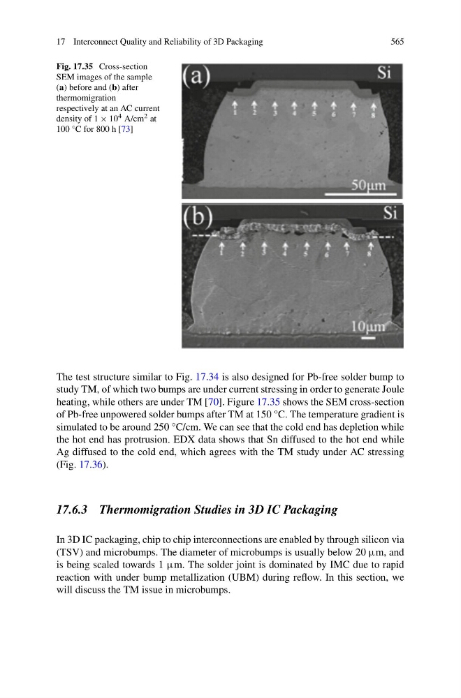
Fig. 17.35 Cross-section
SEM images of the sample
(a) before and (b) after
thermomigration
respectively at an AC current
density of 1 × 10 4 A/cm 2 at
100 °C for 800 h [73]
The test structure similar to Fig. 17.34 is also designed for Pb-free solder bump to
study TM, of which two bumps are under current stressing in order to generate Joule
heating, while others are under TM [70]. Figure 17.35 shows the SEM cross-section
of Pb-free unpowered solder bumps after TM at 150 °C. The temperature gradient is
simulated to be around 250 °C/cm. We can see that the cold end has depletion while
the hot end has protrusion. EDX data shows that Sn diffused to the hot end while
Ag diffused to the cold end, which agrees with the TM study under AC stressing
(Fig. 17.36).
17.6.3 Thermomigration Studies in 3D IC Packaging
In 3D IC packaging, chip to chip interconnections are enabled by through silicon via
(TSV) and microbumps. The diameter of microbumps is usually below 20 μm, and
is being scaled towards 1 μm. The solder joint is dominated by IMC due to rapid
reaction with under bump metallization (UBM) during reflow. In this section, we
will discuss the TM issue in microbumps.
565
Fig. 17.35 Cross-section
SEM images of the sample
(a) before and (b) after
thermomigration
respectively at an AC current
density of 1 × 10 4 A/cm 2 at
100 °C for 800 h [73]
The test structure similar to Fig. 17.34 is also designed for Pb-free solder bump to
study TM, of which two bumps are under current stressing in order to generate Joule
heating, while others are under TM [70]. Figure 17.35 shows the SEM cross-section
of Pb-free unpowered solder bumps after TM at 150 °C. The temperature gradient is
simulated to be around 250 °C/cm. We can see that the cold end has depletion while
the hot end has protrusion. EDX data shows that Sn diffused to the hot end while
Ag diffused to the cold end, which agrees with the TM study under AC stressing
(Fig. 17.36).
17.6.3 Thermomigration Studies in 3D IC Packaging
In 3D IC packaging, chip to chip interconnections are enabled by through silicon via
(TSV) and microbumps. The diameter of microbumps is usually below 20 μm, and
is being scaled towards 1 μm. The solder joint is dominated by IMC due to rapid
reaction with under bump metallization (UBM) during reflow. In this section, we
will discuss the TM issue in microbumps.